Understanding the MC34063: A Comprehensive Guide to DC-DC Conversion
MC34063 is a general-purpose switching regulator chip with functions such as DC-DC conversion, step-up and step-down, and inverting output. It has the advantages of high efficiency, small size, complete functions and low price. This article will introduce its specific information to help you better understand and use this device.Catalog
What is MC34063?

MC34063 is a monolithic integrated circuit that integrates the control circuit of a DC/DC converter. The integrated circuit consists of a reference voltage generator with automatic temperature compensation function, a comparator, a flip-flop, a duty cycle controllable oscillator, and a high current output switching circuit. MC34063 requires only a few switching components to construct boost conversion switches, buck conversion switches and voltage reverse circuits. Compared with linear regulated power supplies, this switching power supply has higher efficiency, and its efficiency will not decrease when the input-output voltage difference is large. At the same time, since it does not require a large radiator and its volume is small, it has a wide range of applications, mainly in systems based on microprocessors or microcontrollers.
Pin diagram and functions of MC34063
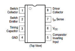
The chip mainly consists of the following eight pins:
• Pin 1: It is the output of the chip. In boost mode, it will provide a high voltage output; in buck mode, it will provide a low voltage output. To ensure output stability, a capacitor needs to be connected to this pin.
• Pin 2: It is the feedback input of the chip. By changing its voltage, the output voltage can be controlled.
• Pin 3: It is the switching output of the chip and is connected to an external switch or diode to generate high-frequency pulses.
• Pin 4: It is the GND terminal of the chip and needs to be connected to ground.
• Pin 5: It is the comparator input of the chip. Through the comparator, the chip can detect the difference between the feedback signal and the reference voltage.
• Pin 6: It is the reference voltage input of the chip. It is an internal 1.25V reference voltage and is used for the comparator.
• Pin 7: It is the power input terminal of the chip and needs to be connected with an electrolytic capacitor to smooth the input voltage.
• Pin 8: It is the switching input of the chip and needs to be connected with a frequency control capacitor and a resistor to control the switching output frequency.
How does MC34063 work?
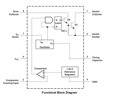
The internal structure of MC34063 is shown in the figure above. The oscillator continuously charges and discharges the timing capacitor externally connected to the CT pin (pin 3) through a constant current source, thereby generating an oscillation waveform. When the load remains constant, the charging and discharging currents are both constant. At this time, the oscillation frequency only depends on the capacity of the external timing capacitor. In the figure above, one end of the AND gate is connected to the output of the oscillator. When the external charge of the oscillator reaches a certain threshold level, the oscillator output flips to high level. The other end of the AND gate is connected to the output end of the comparator. When the voltage at the inverting input end of the comparator is lower than 1.25V, the comparator outputs a high level. When both input terminals of the AND gate become high level, the flip-flop is set to high level and the output switch is turned on; conversely, when the oscillator capacitor outputs low level during discharge, the flip-flop is reset. The output switch tube is in a closed state.
The current limiting function is implemented by detecting the voltage drop on the sampling resistor connected between VCC (pin 6) and pin 7. Once the voltage drop across the resistor is detected to reach 300mV, the current limit circuit will force the oscillator's charging process to change into a discharging process, causing the oscillator's output to become low level, thereby resetting the trigger and turning off the output switch tube.
MC34063 boost circuit calculation method
Output current: MC34063 can provide different output current ranges according to the selection of external components. Based on the requirements of the application, we select appropriate components and parameters.
Capacitor selection: In the boost circuit, the output capacitor is used to smooth the output voltage and provide necessary energy storage. By calculating the variation range of the output current and output voltage, an appropriate output capacitor value can be selected. Larger capacitor values provide lower output ripple but also increase size and cost.
Input voltage and output voltage: First, we need to determine the required input and output voltage. Then, based on the required boost factor and combined with the MC34063 specifications and application notes, we can calculate the required inductor values, capacitor values and parameters of external components.
Inductor selection: According to the specification sheet of MC34063, the required inductance value can be calculated. The selection of the inductor value should take into account factors such as input current, switching frequency and boost multiple. Generally, larger inductor values provide higher boost ratios and lower switching frequencies, but also increase size and cost.
MC34063 step-down switching circuit
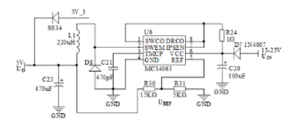
The working principle of the buck circuit is as follows: Pin 5 of the chip monitors the output voltage through external precision resistors R30 and R31. After the output voltage UO is divided, it is input to the inverting input terminal of the comparator together with the voltage UREF. When UREF is lower than the reference voltage, the comparator will output a jump voltage and the S pin of the flip-flop will become high level. During the process of the oscillator charging the capacitor, the R pin is also at a high level, which causes the Q terminal of the flip-flop to become a high level, thereby turning on the output switch. At this time, the input voltage UIN begins to charge the output filter capacitor C23 to increase the output voltage UO, thereby achieving the function of automatically controlling UO stability. On the contrary, when UREF is higher than the reference voltage, the S pin of the flip-flop turns to low level, and the Q terminal also turns to low level, which causes the driver tube Q2 to turn off, and then the switch tube Q1 also turns off. The output voltage is only related to the resistance values of R30 and R31. The calculation formula of the output voltage is:

Among them, the constant 1.25 is the internal reference voltage, which remains constant.
Voltage reverse circuit composed of MC34063
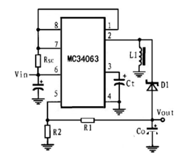
The picture above shows a switching back-voltage circuit composed of MC34063 chip. When the switch T1 inside the chip is turned on, the current flows to the ground through pins 1 and 2 of MC34063 and the inductor LI. At this time, the inductor LI starts to store energy. At the same time, the capacitor Co provides energy to the load. When T1 is turned off, since the current flowing through the inductor cannot change suddenly, the freewheeling diode D1 will conduct. At this time, the inductor Ll supplies power to the load and capacitor Co through D1 (via the common ground), and outputs a negative voltage. As long as the operating frequency of the chip is high enough relative to the time constant of the load, a continuous DC voltage can be obtained on the load.
Advantages of MC34063
MC34063 has the following advantages:
Single-chip solution: MC34063 is a single-chip solution that integrates switching tubes, control circuits and regulating circuits, simplifying the design process and reducing system costs.
Adjustable output voltage: MC34063 supports adjustable output voltage. Users can adjust the output voltage through external components to meet the needs of different applications.
Overload and short-circuit protection: The chip has built-in overload and short-circuit protection functions, which can effectively protect the circuit from external load transient changes or faults, improving the stability and reliability of the system.
High-efficiency conversion: The chip adopts switching regulation technology and has high-efficiency characteristics. It can achieve high-efficiency energy conversion under different input and output voltage conditions and reduce energy loss.
Wide range of applications: MC34063 can be used in a variety of power management and regulation circuits, such as DC-DC converters, inverters, charge pumps, etc., and is suitable for many different electronic equipment and application fields.
Frequently Asked Questions [FAQ]
1. What is a DC to DC boost converter?
A boost converter is a DC to DC converter with an output voltage greater than the source voltage. A boost converter is sometimes called a step-up converter since it "steps up" the source voltage.
2. What is the input voltage of the MC34063?
The input voltage is 5V and the output voltage is 10V or 12V selectable by turning ON the MOSFET connecting the additional resistor.
3. What is the function of the MC34063?
The MC34063 was designed to be incorporated in buck, boost, or voltage-inverter converter applications. All these functions are contained in an 8-pin DIP or SOIC package. The reference voltage is set at 1.25 V and is used to set the output voltage of the converter.
About us
ALLELCO LIMITED
Read more
Quick inquiry
Please send an inquiry, we will respond immediately.
The Role of IMPATT Diodes in Modern Electronics
on August 28th
Comparing the W5300 to other Ethernet controllers: insight into performance and applications
on August 27th
Popular Posts
-
What is GND in the circuit?
on January 1th 3036
-

RJ-45 Connector Guide: RJ-45 Connector Color Codes, Wiring Schemes, R-J45 Applications, RJ-45 Datasheets
on January 1th 2607
-

Fiber Connector Types: SC Vs LC And LC Vs MTP
on January 1th 2162
-
Understanding Power Supply Voltages in Electronics VCC, VDD, VEE, VSS, and GND
on November 13th 2065
-

Comparison Between DB9 and RS232
on January 1th 1789
-

What Is An LR44 Battery?
Electricity, that ubiquitous force, quietly permeates every aspect of our daily lives, from trivial gadgets to life-threatening medical equipment, it plays a silent role. However, truly grasping this energy, especially how to store and efficiently output it, is no easy task. It is against this background that this article will focus on a type of coin cell battery that may seem insignificant on the...on January 1th 1754
-
Understanding the Fundamentals:Inductance Resistance, andCapacitance
In the intricate dance of electrical engineering, a trio of fundamental elements takes center stage: inductance, resistance, and capacitance. Each bears unique traits that dictate the dynamic rhythms of electronic circuits. Here, we embark on a journey to decipher the complexities of these components, to uncover their distinct roles and practical uses within the vast electrical orchestra. Inductan...on January 1th 1704
-

CR2430 Battery Comprehensive Guide: Specifications, Applications and Comparison to CR2032 Batteries
What is CR2430 battery ?Benefits of CR2430 BatteriesNormCR2430 Battery ApplicationsCR2430 EquivalentCR2430 VS CR2032Battery CR2430 SizeWhat to look for when buying the CR2430 and equivalentsData Sheet PDFFrequently Asked Questions Batteries are the heart of small electronic devices. Among the many types available, coin cells play a crucial role, commonly found in calculators, remote controls, and ...on January 1th 1640
-
What Is RF and Why Do We Use It?
Radio Frequency (RF) technology is a key part of modern wireless communication, enabling data transmission over long distances without physical connections. This article delves into the basics of RF, explaining how electromagnetic radiation (EMR) makes RF communication possible. We will explore the principles of EMR, the creation and control of RF signals, and their wide-ranging uses. The article ...on January 1th 1618
-
Comprehensive guide to hFE in transistors
Transistors are crucial components in modern electronic devices, enabling signal amplification and control. This article delves into the knowledge surrounding hFE, including how to select a transistor's hFE value, how to find hFE, and the gain of different types of transistors. Through our exploration of hFE, we gain a deeper understanding of how transistors work and their role in electronic circu...on November 13th 1562

