Understanding Power Supply Voltages in Electronics VCC, VDD, VEE, VSS, and GND
In the world of electronics, the terms VCC, VDD, VEE, VSS, and GND are used to describe different power supply voltages that are needed for the operation of various parts within a circuit. Each of these terms represents a specific voltage type with clear roles and connections, which are very important for making sure electronic devices work properly. Understanding these power supply voltages helps anyone involved in designing, building, or fixing electronic circuits. This guide aims to explain these terms clearly, showing what each one means and how it is used in different types of circuits, helping you gain a better understanding of electronic design and operation.Catalog

Figure 1: Relationship between VCC, VDD, VEE, VSS, and GND
Definitions of VCC, VDD, VEE, VSS, and GND
VCC

Figure 2: VCC as the Positive Supply Voltage in BJTs, Amplifiers, and TTL Circuits
VCC stands for Voltage at the Common Collector. It is the positive power supply voltage connected to the collector terminal of bipolar junction transistors (BJTs). In these transistors, a small current at the base controls a larger current flowing from VCC to the emitter. This setup allows the transistor to amplify or switch signals effectively. VCC provides the energy needed for the transistor to operate. Without this positive voltage, the transistor would not be able to function correctly, as it relies on the voltage difference to drive the current through its collector-emitter path. This makes VCC very helpful in circuits that use BJTs for amplification and switching tasks.
VDD
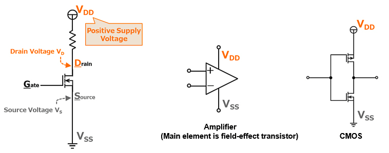
Figure 3: VDD as the Positive Supply Voltage in FETs, Amplifiers, and CMOS Circuits
VDD stands for Voltage at the Drain. It is the positive power supply voltage connected to the drain terminal of field-effect transistors (FETs), especially N-channel FETs. VDD controls the current flow between the drain and source terminals. When a voltage is applied to the gate terminal, it changes the channel's conductivity between the drain and source, allowing the FET to either switch or amplify signals. The value of VDD often determines the maximum voltage the FET can handle, which in turn affects how well the device performs and how efficiently it operates. VDD provides the power for the FET to manage current flow and carry out its switching or amplification functions.
VEE

Figure 4: VEE as the Negative Supply Voltage in BJTs, Amplifiers, and TTL Circuits
VEE is the negative power supply voltage associated with the emitter terminal of BJTs. This voltage is important for the proper operation of the transistor. In an NPN transistor, VEE ensures that the emitter is at a lower potential than the collector, a condition needed for the transistor to conduct correctly. Proper biasing through VEE allows the transistor to maintain a stable operating point, ensuring it functions within its specified voltage range. VEE is often connected to ground or a lower potential, enabling the current to flow from the emitter to the collector, thus allowing the transistor to amplify or switch signals accurately. Without VEE, the transistor would not be able to achieve the required bias conditions for proper operation.
VSS

Figure 5: VSS as the Negative Supply Voltage in FETs, Amplifiers, and CMOS Circuits
VSS stands for Voltage at the Source and is usually the negative supply voltage connected to the source terminal of N-channel FETs. VSS acts as the common ground or reference point for the circuit, ensuring proper voltage levels across the device. It defines the zero voltage level in the circuit, against which all other voltages are measured. This reference point is very helpful for the stable operation of the FET, allowing it to control the current flow between the drain and source terminals effectively. VSS provides the stable baseline that the FET uses to manage current flow and perform its functions reliably. In many circuits, VSS is synonymous with ground, providing a consistent reference point for the entire circuit.
GND

Figure 6: GND as the Common Reference Point in a Circuit
GND stands for Ground. It is the voltage reference point in a circuit. GND serves as the common reference point for all voltage measurements within the circuit, providing a consistent baseline for comparing all other voltages. It is needed for maintaining a stable voltage environment, preventing fluctuations that could affect the operation of the circuit. By providing a consistent reference, GND helps ensure accurate measurements and stable circuit performance, avoiding noise and interference that could disrupt the circuit's operation. GND is the common point where all other voltages in the circuit are referenced, ensuring that the circuit functions smoothly and predictably.
Other Common Power Supply Labels in Electronic Circuits
VBAT (Voltage Battery) is a voltage used to keep backup registers and the Real-Time Clock (RTC) running when the main power supply (VDD) is off. This means that even if the main power source is not available, important functions like keeping the memory and time continue to work. This ensures that devices like clocks keep showing the right time and data is saved, even when the main power is off. This is very helpful in making sure these devices work all the time, much like how consistent and reliable support is important for individuals to maintain stability and progress through challenging times.
VPP (Programming Voltage) is the voltage used for programming or erasing memory devices. It supplies the higher voltage needed to alter the stored data in programmable devices like EPROMs (Erasable Programmable Read-Only Memory) and flash memory. This voltage is usually higher than the regular operating voltages to ensure the memory can be properly written or erased. Without VPP, these devices would not be able to update their stored information effectively.
VA (Analog Voltage) indicates the specific voltage level used for analog operations in circuits that have both digital and analog parts. This separation ensures that both types of signals work correctly in the same circuit. By maintaining distinct voltage levels for analog and digital operations, VA helps prevent interference between the two, keeping the signals clear and accurate.
CC (Collector Voltage) and DD (Drain Voltage) represent the difference between the power supply voltage and the working voltage in a circuit, typically with VCC being higher than VDD. VCC is the higher power supply voltage needed for the overall operation of the circuit. VDD, on the other hand, is the lower working voltage needed by specific parts of the circuit. This distinction helps manage power distribution effectively, ensuring that each part of the circuit gets the appropriate voltage for its operation. For example, in some circuits, VCC might be 5V for powering the entire system, while VDD might be 3.3V for certain sensitive components, allowing for efficient and stable performance across different parts of the circuit.
Application Explanation
Understanding how VCC, VDD, VEE, VSS, and GND work in digital circuits is necessary for good circuit design and operation. Each voltage has a specific job to make sure electronic parts work well together.
VCC is the main power supply voltage for the whole circuit. It gives the energy needed to power all parts, making sure they work correctly.
VDD is the working voltage specific to the chip or integrated circuit (IC). It is usually lower than VCC because the chip's internal voltage regulators lower the voltage to the needed level. For example, in ARM microcontrollers, the power supply voltage (VCC) is usually 5V, which is then changed to a working voltage (VDD) of 3.3V through a voltage stabilization module. Some ICs have both VDD and VCC pins, showing that the device can handle different voltage levels. This helps the IC manage power better, making sure of good performance and energy efficiency.
In circuits that use field-effect transistors (FETs) or CMOS devices, VDD is the voltage at the drain terminal of the transistor, while VSS is the voltage at the source terminal. VDD is the positive supply voltage that allows the FET to control current flow, while VSS is the ground point, providing a return path for the current.
Generally, VCC is used to denote the analog power supply, VDD is used for the digital power supply, VSS is the digital ground, and VEE represents the negative power supply. Each of these voltages is needed for different types of circuits and parts, making sure they work correctly within their limits.
In electrical terms, GND, or ground, can be divided into power ground (PG) and signal ground. Power ground is used for high-current devices, providing a stable reference point for heavy loads and making sure of the safe operation of these devices. Signal ground is used for low-current or signal circuits, maintaining a stable reference point for sensitive signal processing parts. Power ground and signal ground have different purposes but are both needed for the overall stability and performance of electronic circuits. Good grounding techniques are needed to minimize noise and interference, making sure that both high-current and low-current circuits work reliably and efficiently.
Bipolar Junction Transistors (BJT)

Figure 7: Bipolar Junction Transistor (BJT) Showing VCC and VEE
Bipolar Junction Transistors (BJTs) are one of the main building blocks of electronic circuits. They come in two types NPN and PNP, with NPN being more common in modern circuits. The names for power supply voltages in BJTs are derived from the specific terminals of the transistor the collector, emitter, and base.
VCC Voltage at the Common Collector
VCC is the positive supply voltage connected to the collector terminal of a BJT, especially in NPN-type transistors. VCC stands for Voltage at the Common Collector, with Common showing that this voltage is shared across many transistors in a circuit. The double CC makes it clear that this is a power supply voltage and not just a single point voltage (VC).
VCC is needed for BJTs because it provides the potential difference that allows current to flow from the collector to the emitter. This current flow is what allows the transistor to work as an amplifier or a switch. In amplification, the transistor uses VCC to boost the strength of the input signal. In switching, VCC helps turn the transistor on and off, controlling the current flow through the circuit.
For example, in a common-emitter amplifier setup, VCC is connected through a load resistor to the collector. The input signal at the base changes the current flow from the collector to the emitter, allowing the transistor to amplify the input signal. VCC provides the power needed for this amplification.
VEE Voltage at the Emitter
VEE is the negative supply voltage connected to the emitter terminal of a BJT, especially in NPN-type transistors. VEE stands for Voltage at the Emitter, and the double EE separates it from other emitter-related voltages (VE).
VEE is needed for correctly biasing the transistor. Biasing means setting the transistor's operating point by applying the correct voltages to its terminals. For an NPN transistor to work correctly, the emitter must be at a lower potential than the collector. This ensures that the base-emitter junction is forward-biased, allowing current to flow from the base to the emitter, while the base-collector junction is reverse-biased, controlling the larger current flow from the collector to the emitter.
In many circuits, VEE is connected to the ground, providing a stable reference point for the emitter. This is common in single power supply systems, where the ground serves as the negative voltage reference for the whole circuit. In these setups, the ground (0V) is the same as VEE.
For example, in a differential amplifier, which is a basic building block in analog circuits, the emitters of two BJTs are connected together and then to the negative supply voltage VEE through a common emitter resistor. This ensures that the transistors are properly biased and can amplify the differential input signal applied to their bases.
Field-Effect Transistors (FET)

Figure 8: Field-Effect Transistor (FET) Showing VDD and VSS
Field-Effect Transistors (FETs) are a kind of transistor used in electronic circuits. There are different types of FETs, with the most common ones being N-channel and P-channel MOSFETs (Metal-Oxide-Semiconductor Field-Effect Transistors). The names for power supply voltages in FETs come from the specific parts of the transistor the drain, source, and gate.
VDD Voltage at the Drain
VDD stands for Voltage at the Drain. This term refers to the positive supply voltage connected to the drain part of an N-channel FET. The DD in VDD shows it as a power supply voltage.
VDD voltage goes to the drain of an N-channel FET. For the FET to work correctly, the drain needs to be at a higher voltage than the source. This allows current to move from the drain to the source when voltage is applied to the gate, controlling the flow of current between the drain and source. VDD gives the needed power for the FET to control current flow and perform its switching or amplifying functions. In CMOS circuits, VDD powers the digital logic gates, helping them to process and send digital signals.
VSS Voltage at the Source
VSS stands for Voltage at the Source. This term refers to the negative supply voltage connected to the source part of an N-channel FET. The SS in VSS shows it as a power supply voltage.
VSS voltage goes to the source of an N-channel FET. For the FET to work correctly, the source needs to be at a lower voltage than the drain. This setup makes sure the FET can control the current flow between the drain and source parts effectively. VSS often acts as the ground reference in these circuits, giving a stable reference point for the FET's operation. By defining the zero voltage level in the circuit, VSS helps maintain the proper voltage levels across the device, allowing it to work reliably.
6. Differences and Examples of VCC, VDD, VEE, VSS, and GND in Electronics
VBAT (Voltage Battery) is a voltage used to keep backup registers and the Real-Time Clock (RTC) running when the main power supply (VDD) is off. This means that even if the primary power source is unavailable, basic functions like memory retention and timekeeping continue to work. This is helpful in applications that need continuous operation, such as maintaining the time in a clock or preserving data in memory.
VCC
• Usage VCC is the positive supply voltage for circuits using bipolar junction transistors (BJTs) and operational amplifiers. It provides the energy needed to power these components.
• Collector Connection VCC is directly connected to the collector terminal of NPN-type BJTs. This connection supplies the voltage required for the transistor to work correctly. The collector needs to be at a higher potential than the emitter to allow current to flow from the collector to the emitter. This is needed for the transistor's amplification and switching operations. In operational amplifiers, VCC supplies the power needed for the op-amp to operate within its intended voltage range, enabling it to amplify signals accurately.
VEE
• Usage VEE serves as the negative supply voltage for circuits using BJTs and operational amplifiers. It provides a lower potential point in the circuit.
• Emitter Connection VEE is directly connected to the emitter terminal of NPN-type BJTs. This ensures that the emitter is correctly biased with a negative voltage, which is needed for the proper operation of the transistor. The emitter must be at a lower potential than the base for the transistor to conduct properly. In many circuit designs, VEE is connected to the ground or a lower potential than the ground, helping the transistor to work correctly. This setup allows for stable current flow and accurate signal amplification or switching.
VDD
• Usage VDD is the positive supply voltage used in circuits that employ field-effect transistors (FETs) and complementary metal-oxide-semiconductor (CMOS) technology. It powers the internal circuits and logic gates of these devices.
• Drain ConnectionVDD is directly connected to the drain terminal of N-channel FETs. This connection supplies the required voltage for the drain, allowing the FET to control the current flow between the drain and source. The drain must be at a higher voltage than the source for current to flow from the drain to the source. In CMOS circuits, VDD provides the power needed for the digital logic gates to work correctly, enabling the processing and transmission of digital signals.
VSS
• Usage VSS represents the negative supply voltage in circuits with FETs and CMOS devices. It serves as the reference point for the source terminal in these devices.
• Source Connection VSS is directly connected to the source terminal of N-channel FETs. This ensures that the source is at a lower potential compared to the drain, which is needed for the FET to work correctly. VSS often serves as the ground reference in these circuits, maintaining the stability and proper functioning of the FET and CMOS devices. By providing a stable reference point, VSS helps ensure consistent performance and reliable operation of the transistors and logic gates within the circuit.
GND (Power Ground and Signal Ground)
GND, or ground, is the voltage reference point in a circuit. It acts as a common return path for electric current and helps keep a stable voltage environment within the circuit.
• Power Ground Used for high-current network devices and power amplifiers, power ground provides a stable reference for high-power circuits. This type of ground ensures that the high currents in power circuits do not interfere with the sensitive components in the circuit.
• Signal Ground Used for low-current or signal circuits, signal ground ensures a noise-free reference point for sensitive signal processing components. Proper grounding techniques are needed to minimize noise and interference, which can degrade the performance of the circuit. By providing a stable reference point, signal ground helps to ensure accurate signal transmission and processing.
Conclusion
Knowing and using VCC, VDD, VEE, VSS, and GND correctly is very helpful for designing and operating electronic circuits successfully. VCC is the positive supply voltage for bipolar junction transistors and operational amplifiers, making sure these parts have the power they need to work. VDD is the positive supply voltage for field-effect transistors and CMOS devices, controlling the current flow needed for their operation. VEE and VSS provide the needed negative voltages for BJTs and FETs, setting the correct bias and reference points for stable performance. GND, or ground, is the common reference point for all voltages in a circuit, ensuring stability and preventing fluctuations that could disrupt the circuit's operation.
By understanding the specific roles and connections of these voltages, you can design more reliable and efficient circuits. Each voltage type has a distinct purpose, helping the electronic parts work together smoothly. With this knowledge, you can better solve problems, improve circuit performance, and make sure all parts work together seamlessly.
Frequently Asked Questions [FAQ]
1. What is the difference between VCC and VEE?
VCC and VEE are different power supply voltages in circuits using bipolar junction transistors (BJTs). VCC is the positive voltage connected to the collector terminal of NPN-type BJTs. It allows current to flow from the collector to the emitter, letting the transistor amplify or switch signals. VEE is the negative voltage connected to the emitter terminal of BJTs. It makes sure the emitter is at a lower potential than the collector, which is needed for the transistor to work properly. VEE helps set the right conditions for stable operation.
2. What voltage is GND?
GND, or ground, is typically set at 0 volts. It serves as the common reference point for all other voltages in an electronic circuit. This means that all other voltages are measured relative to GND, ensuring a stable voltage environment within the circuit.
3. What does GND stand for?
GND stands for ground. In electronic circuits, it acts as the reference point for all voltage measurements. It provides a common return path for electric current, which helps maintain stability and prevent voltage changes that could affect the circuit's operation.
4. What is VCC, VDD, and VSS?
VCC, VDD, and VSS are types of power supply voltages in electronic circuits. VCC is the positive voltage for bipolar junction transistors (BJTs) and operational amplifiers, providing energy for their operation. VDD is the positive supply voltage for field-effect transistors (FETs) and CMOS technology, powering internal circuits and logic gates. VSS is the negative supply voltage or ground reference for FETs and CMOS devices, acting as the reference point for stable operation.
5. Is VSS or VDD positive?
VDD is positive. It serves as the positive supply voltage in circuits using field-effect transistors (FETs) and CMOS technology, powering the internal circuits and logic gates. VSS, on the other hand, is usually the ground or negative reference point, providing the stable reference voltage needed for the operation of these devices.