
Manufacturer Part Number
NTGD3133PT1G
Manufacturer
onsemi
Introduction
Dual P-Channel MOSFET
Product Features and Performance
Drain to Source Voltage (Vdss) of 20V
RDS(on) of 145mΩ @ 2.2A, 4.5V
Continuous Drain Current (ID) of 1.6A @ 25°C
Input Capacitance (Ciss) of 400pF @ 10V
Gate Charge (Qg) of 5.5nC @ 4.5V
Logic Level Gate
Wide Operating Temperature Range of -55°C to 150°C
Power Dissipation of 560mW
Product Advantages
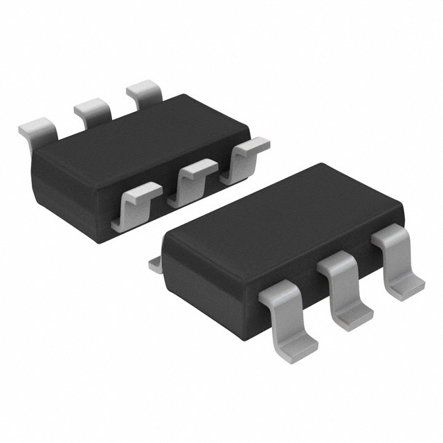
Compact SOT-23-6 package
Dual P-Channel configuration for space-saving designs
Low on-resistance for improved efficiency
Logic Level Gate for easy interface with microcontrollers
Key Technical Parameters
Drain to Source Voltage (Vdss): 20V
RDS(on) (Max) @ Id, Vgs: 145mΩ @ 2.2A, 4.5V
Continuous Drain Current (ID) @ 25°C: 1.6A
Input Capacitance (Ciss) (Max) @ Vds: 400pF @ 10V
Gate Charge (Qg) (Max) @ Vgs: 5.5nC @ 4.5V
Vgs(th) (Max) @ Id: 1.4V @ 250μA
Quality and Safety Features
AEC-Q101 qualified for automotive applications
RoHS compliant for environmental responsibility
Compatibility
Compatible with various microcontrollers and control circuits
Application Areas
Power management
Motor control
Lighting control
General-purpose switching
Product Lifecycle
Currently in active production
Replacement or upgraded models may be available in the future
Several Key Reasons to Choose This Product
Compact and space-saving dual P-Channel MOSFET configuration
Low on-resistance for improved power efficiency
Wide operating temperature range for versatile applications
Logic Level Gate for easy microcontroller integration
AEC-Q101 qualification for automotive and industrial use
RoHS compliance for environmental considerations

 NTGS3441AMI Semiconductor/onsemi