NMOS and PMOS Guide - How it Works, Pros and Cons, Applications, Truth Tables, Comparison of the Two
Catalog
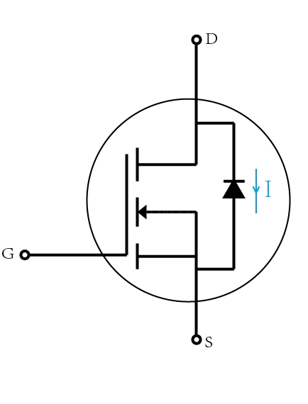
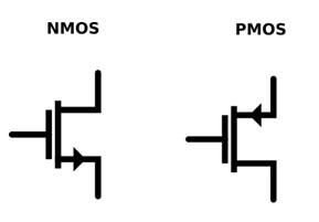
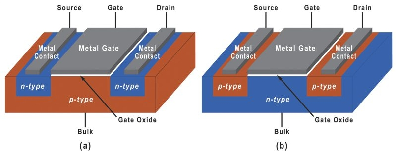
1. Definition and working principle of NMOS transistor
2. Technical advantages and disadvantages of NMOS transistors
2.1 Advantages of NMOS transistors:
2.2 Disadvantages of NMOS transistors:
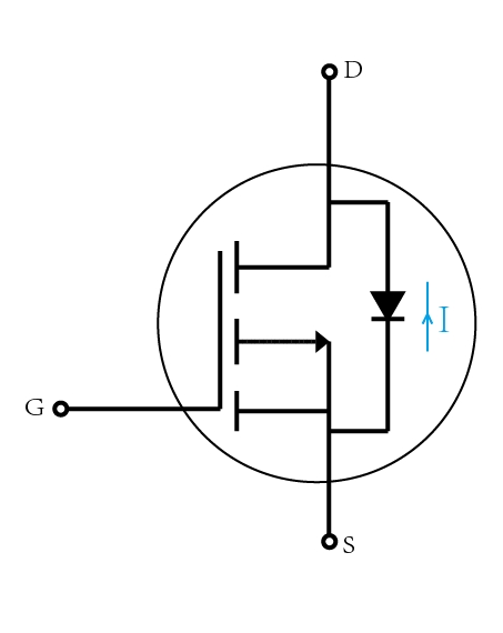
3. Definition and working principle of PMOS transistor
4. Technical advantages and disadvantages of PMOS transistors
4.1 Advantages of PMOS Transistors:
4.2 Disadvantages of PMOS transistors:
5. NMOS and PMOS: truth table
|
Gate Voltage (V_Gs) |
Souree-Drain Current (l Ds) |
Transistor State |
|
High (Logic 1) |
High |
ON |
|
Low (Logic 0) |
LOW |
OFF |
6. Comparison between NMOS and PMOS
|
Aspect |
NMOS (N-type
Metal-Oxide-Semiconductor) |
PMOS (P-type
Metal-Oxide-Semiconductor) |
|
Majority Charge Carriers |
Electrons |
Holes (Positive Charge Carriers) |
|
Semiconductor Type |
n-type |
p-type |
|
Gate Voltage Control |
Positive Voltage |
Positive Voltage |
|
Operation |
Conducts when Gate is Positive |
Conducts when Gate is Negative |
|
Switching Speed |
Faster Switching Speed |
Slower Switching Speed |
|
Power Consumption |
Higher Power Consumption |
Lower Power Consumption |
|
Noise Immunity |
Lower Noise Immunity |
Higher Noise Immunity |
|
Applications |
High-Speed Digital Circuits,
Microprocessors, Memory Cells, Integrated Circuits |
Low-Power Digital Circuits, CMOS
Technology, Analog Amplifiers, Voltage Level Shifters, Power Management
Circuits |
7. NMOS and PMOS: Which one is better?
8. Conclusion
Frequently Asked Questions [FAQ]
1. What would happen if we interchanged PMOS and NMOS?
2. Which is better, NMOS or PMOS current source?
3. Which is bigger, NMOS or PMOS?
4. Does PMOS have higher resistance than NMOS?
About us
ALLELCO LIMITED
Read more
Quick inquiry
Please send an inquiry, we will respond immediately.
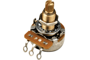
What Is the Function of a Potentiometer?
on May 8th
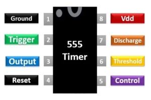
Mastering the 555 Timer: Principles, Modes, Applications, and Practical Implementation
on May 7th
Popular Posts
-
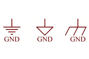
What is GND in the circuit?
on January 1th 3254
-

RJ-45 Connector Guide: RJ-45 Connector Color Codes, Wiring Schemes, R-J45 Applications, RJ-45 Datasheets
on January 1th 2801
-
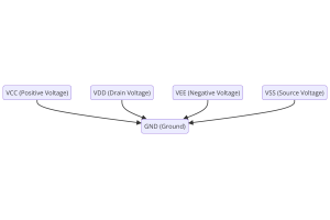
Understanding Power Supply Voltages in Electronics VCC, VDD, VEE, VSS, and GND
on November 19th 2608
-

Fiber Connector Types: SC Vs LC And LC Vs MTP
on January 1th 2250
-

Comparison Between DB9 and RS232
on January 1th 1867
-

What Is An LR44 Battery?
Electricity, that ubiquitous force, quietly permeates every aspect of our daily lives, from trivial gadgets to life-threatening medical equipment, it plays a silent role. However, truly grasping this energy, especially how to store and efficiently output it, is no easy task. It is against this background that this article will focus on a type of coin cell battery that may seem insignificant on the...on January 1th 1836
-
Understanding the Fundamentals:Inductance Resistance, andCapacitance
In the intricate dance of electrical engineering, a trio of fundamental elements takes center stage: inductance, resistance, and capacitance. Each bears unique traits that dictate the dynamic rhythms of electronic circuits. Here, we embark on a journey to decipher the complexities of these components, to uncover their distinct roles and practical uses within the vast electrical orchestra. Inductan...on January 1th 1791
-
What Is RF and Why Do We Use It?
Radio Frequency (RF) technology is a key part of modern wireless communication, enabling data transmission over long distances without physical connections. This article delves into the basics of RF, explaining how electromagnetic radiation (EMR) makes RF communication possible. We will explore the principles of EMR, the creation and control of RF signals, and their wide-ranging uses. The article ...on January 1th 1780
-
CR2430 Battery Comprehensive Guide: Specifications, Applications and Comparison to CR2032 Batteries
What is CR2430 battery ?Benefits of CR2430 BatteriesNormCR2430 Battery ApplicationsCR2430 EquivalentCR2430 VS CR2032Battery CR2430 SizeWhat to look for when buying the CR2430 and equivalentsData Sheet PDFFrequently Asked Questions Batteries are the heart of small electronic devices. Among the many types available, coin cells play a crucial role, commonly found in calculators, remote controls, and ...on January 1th 1775
-
Comprehensive guide to hFE in transistors
Transistors are crucial components in modern electronic devices, enabling signal amplification and control. This article delves into the knowledge surrounding hFE, including how to select a transistor's hFE value, how to find hFE, and the gain of different types of transistors. Through our exploration of hFE, we gain a deeper understanding of how transistors work and their role in electronic circu...on November 19th 1761
HOT Part Number
-

PI6C10807HE
Diodes Incorporated
IC CLK BUFFER 1:10 250MHZ 20SSOP
SMCJ5.0A-13-F
Diodes Incorporated
TVS DIODE 5VWM 9.2VC SMC
EL1503ACLZ
Renesas Electronics America Inc
IC DRIVER 2/0 24QFN
UPA2004GR-A
Renesas Electronics America Inc
DARLINGTON TRANSISTOR ARRAY
W25Q16BVSSIG
Winbond Electronics
IC FLASH 16MBIT SPI/QUAD 8SOIC
THVD1510DGK
Texas Instruments
IC TRANSCEIVER HALF 1/1 8VSSOP
LT1009CLPE3
Texas Instruments
IC VREF SHUNT 0.2% TO92-3
GRM2165C1H242JA01D
Murata Electronics
CAP CER 2400PF 50V C0G/NP0 0805
APA1606CGCK
Kingbright
LED GREEN CLEAR CHIP SMD R/A
AH276UZ4-CG1
Diodes Incorporated
MAGNETIC SWITCH LATCH TO94
08052C561KAT4A
KYOCERA AVX
CAP CER 560PF 200V X7R 0805
IRF3515S
Infineon Technologies
MOSFET N-CH 150V 41A D2PAK
LTC3310SIV-1#TRMPBF
Analog Devices Inc.
10A LOW VLTG SYNCH STEP-DWN SILN
MAX448ACSD
Analog Devices Inc./Maxim Integrated
IC OPAMP GP 4 CIRCUIT 14SOIC
MCF51JM128VLD
NXP USA Inc.
IC MCU 32BIT 128KB FLASH 44LQFP
HVU306ATRU-E
Renesas Electronics America Inc
VARIABLE CAPACITANCE DIODE, VERY
CD74HCT174M96
Harris Corporation
IC FF D-TYPE SNGL 6BIT 16SOIC
LTC3728EUH#PBF
Analog Devices Inc.
IC REG CTRLR BUCK 32QFN -

MAX8511EXK26+T
Analog Devices Inc./Maxim Integrated
IC REG LINEAR 2.6V 120MA SC70-5
MC100EL05DR2
onsemi
IC GATE AND/NAND ECL 2INP 8-SOIC
SDV1005E140C500NPTF
Shenzhen Sunlord Electronics Co., Ltd.
VARISTOR 22V 10A 0402
FERD40H100SG-TR
STMicroelectronics
DIODE FERD 100V 40A D2PAK
LTC4401-1ES6#TRPBF
ADI (Analog Devices, Inc.)
IC RF PWR CNTRL 2.7GHZ TSOT23-6
STM32F101RET6
STMicroelectronics
IC MCU 32BIT 512KB FLASH 64LQFP
NDP603AL
Fairchild Semiconductor
MOSFET N-CH 30V 25A TO220-3
V300LA20CP
Hamlin / Littelfuse
VARISTOR 470V 6.5KA DISC 14MM
APD2220-000
Skyworks Solutions Inc.
RF DIODE PIN 100V DIE
T491X157K016AT
KEMET
CAP TANT 150UF 10% 16V 2917
LT6200IS6-10#TRM
Analog Devices Inc.
IC BUFFER 1 CIRCUIT TSOT23-6
CASR 25-NP
LEM USA Inc.
SENSOR CURRENT FLUX 25A AC/DC
BQ25121YFPR
Texas Instruments
IC BATT CHG LI-ION 1CELL 25DSBGA
TSI572-10GILV
Renesas Electronics America Inc
IC SER RAPIDIO SWITCH 399TEPBGA
SI8641BB-AS1
Skyworks Solutions Inc.
AUTOMOTIVE 2.5 KV 3 FORWARD & 1
MCIMX353DJQ5C
NXP USA Inc.
IC MPU I.MX35 532MHZ 400MAPBGA
MCIMX27LVOP4A
NXP USA Inc.
IC MPU I.MX27 400MHZ 404MAPBGA
VE-251-IV
Vicor Corporation
DC DC CONVERTER 12V 150W -

TSV631IYLT
STMicroelectronics
IC OPAMP GP 1 CIRCUIT SOT23-5
RS2102XN
Runic Technology
IC SWITCH SPDT X 2 4OHM 10MSOP
HUF75339P3
Harris Corporation
MOSFET N-CH 55V 75A TO220-3
SPH252010H220MT
Shenzhen Sunlord Electronics Co., Ltd.
FIXED IND 22UH 400MA 1.548OHM SM
A8508GLPTR-T
Allegro MicroSystems
IC LED DRIVER CTRLR PWM 24TSSOP
S9S12G48F0MLF
NXP USA Inc.
IC MCU 16BIT 48KB FLASH 48LQFP
TMS320C6204ZHKA200
Texas Instruments
IC FIXED-POINT DSP 288-BGA
LT8619EMSE-5#TRPBF
Analog Devices Inc.
IC REG BUCK 5V 1.2A 16MSOP
LM35CAZ
Texas Instruments
ANALOG VOLTAGE OUTPUT SENSOR, -.
1812GC100KAT1A\SB
KYOCERA AVX
CAP CER 10PF 2KV X7R 1812
ATMEGA1281V-8AU
Microchip Technology
IC MCU 8BIT 128KB FLASH 64TQFP
5KP18CA
Diotec Semiconductor
TVS D8X7.5 18V 5000W BI
NID5003NT4G
onsemi
IC PWR DRIVER N-CHANNEL 1:1 DPAK
PI5C3244Q
Diodes Incorporated
IC BUS SWITCH 4 X 1:1 20QSOP
046227004100800+
KYOCERA AVX
CONN FFC FPC 4POS 1MM R/A
LT4320IMSE-1#TRPBF
Analog Devices Inc.
IC OR CTRLR BRIDGE RECT 12MSOP
95V857AGILF
Renesas Electronics America Inc
IC CLK BUF DDR 233MHZ 1CIRC
1N914BWS
onsemi
DIODE GEN PURP 75V 150MA SOD323F