A Complete Guide to Understanding Bipolar Junction Transistors (BJT)
Bipolar junction transistors (BJTs) are fundamental to modern electronics, playing a key role in amplification and switching operations in a wide variety of applications. Central to their functionality lies the ability to control the movement of electrons and holes within semiconductor materials, a principle that depends on the complexity of P-type and N-type materials and their interaction at the PN junction. This article delves into the detailed structure, operation, and practical applications of BJTs, exploring both PNP and NPN configurations. From the microscopic interactions within the base, emitter, and collector regions to the macroscopic applications in devices ranging from simple audio amplifiers to complex digital circuits, BJTs embody a perfect synergy between physics and function. By considering their operating mechanisms as well as their configuration, we can understand the necessary role that BJTs play in enhancing signal integrity, managing power levels, and ensuring high precision in state switching.Catalog
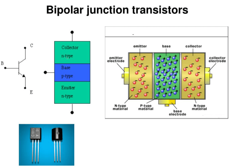
Figure 1: Bipolar Junction Transistors
Exploring the Function of Bipolar Junction Transistors
Bipolar Junction Transistors (BJTs) are needed in electronics for amplification and switching. To understand their practical use, it helps to know some basics of semiconductors, including the differences between P-type and N-type materials and how PN junctions work. BJTs regulate current by controlling the movement of electrons and holes.
BJTs are key in designing efficient amplifiers. They amplify weak signals, making them useful in audio devices, medical equipment, and telecommunications. For example, in an audio amplifier, a BJT can boost sound signals from a mobile device to drive speakers, providing clear and loud audio.
In switching applications, BJTs manage logic operations in digital circuits and control power flow in power systems. During a switching operation, a BJT quickly alternates between cutoff and saturation states, acting as an electronic switch to control power in devices like computers and smart appliances.
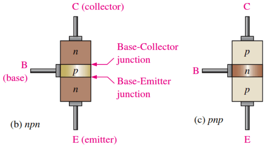
Figure 2: Bipolar Junction Transistors (BJTs) Structure
The Structure of Bipolar Junction Transistors (BJT)
A Bipolar Junction Transistor (BJT) is a fundamental component in electronics, composed of three layers of semiconductor material. These layers are configured either as P-N-P or N-P-N, each with a specific doping pattern. The outer layers are the emitter and collector, while the central layer acts as the base. Each layer is connected to external circuits through metallic leads, allowing the BJT to be integrated into various electronic systems.
BJTs function primarily as current-controlled devices, capable of controlling and amplifying electrical currents. In operation, the emitter introduces charge carriers (electrons in NPN, holes in PNP) into the base, where these carriers are in the minority. The base is deliberately made thin and lightly doped to allow most of these carriers to pass through to the collector without recombining. The collector, larger and more heavily doped, captures these carriers to handle higher currents and voltages.
For effective operation, BJTs require appropriate biasing with external voltages applied to their terminals. The emitter-base junction is forward-biased to facilitate the flow of carriers, while the collector-base junction is reverse-biased to block carrier flow. This arrangement enables a small base current to control a much larger collector-emitter current. The ratio of these currents, known as the current gain, is key for BJT applications. The current flow direction in BJTs depends on the type of transistor. In NPN transistors, electrons flow from the emitter to the collector, whereas in PNP transistors, holes travel from the emitter to the collector. The direction of conventional current flow is indicated by an arrow on the emitter leg in the transistor's schematic symbol: outward for NPN and inward for PNP.
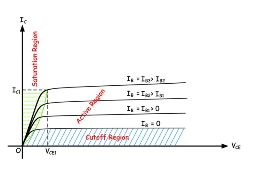
Figure 3: Operational Regions of Bipolar Junction Transistors
How Bipolar Junction Transistors Work?
Bipolar Junction Transistors (BJTs) operate in three primary regions: active, saturation, and cut-off. Each region is defined by the bias conditions of the emitter-base and collector-base junctions, which directly affect the transistor's role in circuits.
Active region: the emitter-base junction is forward-biased, and the collector-base junction is reverse-biased. This configuration allows BJTs to function as linear amplifiers. Here, a small change in the base current results in a much larger change in the collector current. This property is required for signal amplification, where the transistor boosts an input signal into a significantly larger output without reaching full conductivity.
Saturation region: both the emitter-base and collector-base junctions are forward-biased. This puts the transistor in a fully "on" state, similar to a closed switch, where the collector current is maximized, approaching its saturation limit. This region is settling for digital electronics, where transistors need to switch on and off rapidly, providing clear and distinct signals for binary logic operations.
Cut-off region: both junctions are reverse-biased, turning the transistor completely "off." In this state, the collector current drops to zero, similar to an open switch. This condition is needed for controlling circuit pathways in digital applications, ensuring no current flows when the transistor is intended to be off.
Various Types of Bipolar Junction Transistors: Characteristics and Uses
Bipolar Junction Transistors (BJTs) are categorized into two main types based on their doping arrangements and current flow direction: PNP and NPN. Each type has unique structural and operational characteristics that suit specific applications.
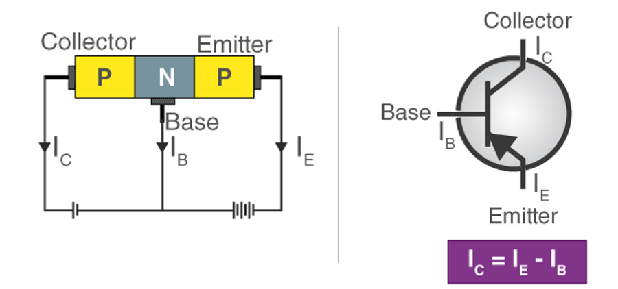
Figure 4: PNP Bipolar Junction Transistor
PNP BJT
In PNP transistors, the central N-type layer is sandwiched between two P-type layers, acting as the emitter and collector. In this configuration, holes are the primary charge carriers. When the emitter-base junction is forward-biased, holes flow from the emitter into the base. Since the base is thin and lightly doped, most holes pass through to the collector, which is reverse-biased, preventing electron flow in the opposite direction. This setup allows for effective current amplification, where a small base current controls a much larger current from the emitter to the collector.
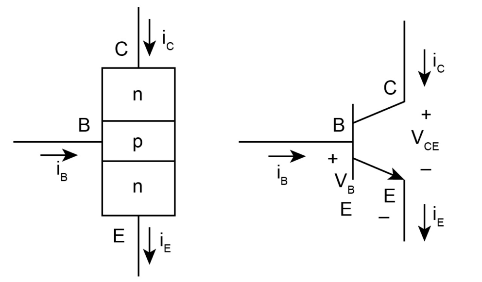
Figure 5: NPN Bipolar Junction Transistor
NPN BJT
NPN transistors have a central P-type layer flanked by N-type materials. Here, electrons are the primary charge carriers. Forward-biasing the emitter-base junction enables electrons to flow from the emitter into the base. As in the PNP type, the reverse-biased collector-base junction blocks hole flow from the collector to the base, allowing a larger electron flow from the emitter to the collector. NPN transistors are particularly effective in applications that require high electron mobility, such as high-speed switching and amplification circuits.
In both PNP and NPN transistors, the direction of current flow (conventional current, from positive to negative) and the type of charge carriers are key for understanding how BJTs control and amplify current.
Configurations and Settings of Bipolar Transistors
Bipolar Junction Transistors (BJTs) can be used in three main configurations in electronic circuits: common base, common emitter, and common collector. Each configuration has unique electrical characteristics suited to different applications.
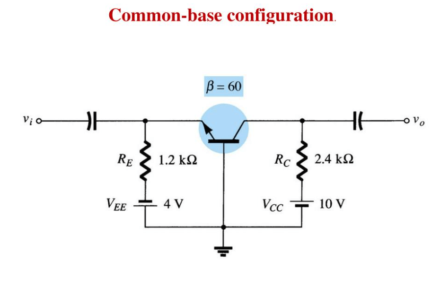
Figure 6: Common Base Configuration
Common Base (CB) Configuration
In the common base configuration, the base terminal is shared between the input and output circuits, acting as a ground for AC signals. This setup provides high voltage gain but minimal current gain, making it ideal for applications needing stable voltage amplification, like RF amplifiers. Here, the base current doesn't influence the output, ensuring consistent performance even with variable signal conditions.
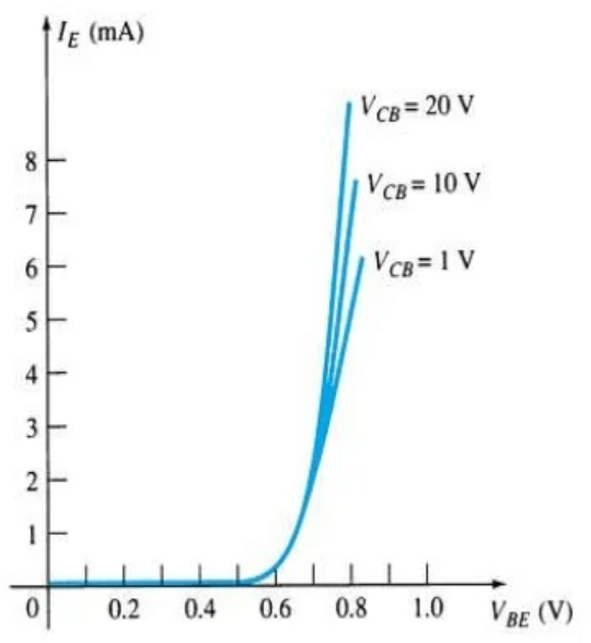
Figure 7: Common Base Input Characteristics
In a common base transistor configuration, the analysis of input characteristics examines how the emitter current (IE) varies with changes in the base-emitter voltage (VBE) while keeping the collector-base voltage (VCB) constant. Typically, VBE is plotted on the x-axis against IE on the y-axis. Starting with a VCB of zero volts, an increase in VBE leads to a corresponding rise in IE, depicting the relationship between input voltage and current when the output voltage is fixed. As VCB is raised to a higher stable value, like 8 volts, and VBE increases from zero, the input characteristics curve shifts due to a lower cut-in voltage. This shift results from the narrowing of the depletion region at the emitter-base junction, which is driven by the increased reverse bias at higher VCB levels, thereby enhancing the injection of charge carriers from the emitter into the base.
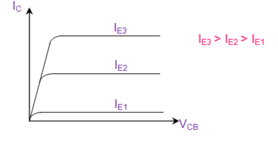
Figure 8: Common Base Output Characteristics
Exploring output characteristics involves studying how the collector current (IC) changes with variations in collector-base voltage (VCB) while keeping the emitter current (IE) constant. Initially, IE is set to zero mA to analyze the transistor in the cut-off region. In this state, increases in VCB have little effect on IC, indicating the transistor is non-conductive.
When IE is increased incrementally, for example to 1 mA, and VCB is varied, the transistor operates in its active region where it acts mainly as an amplifier. The output characteristics are depicted through curves that stay relatively flat as VCB increases with a fixed IE.
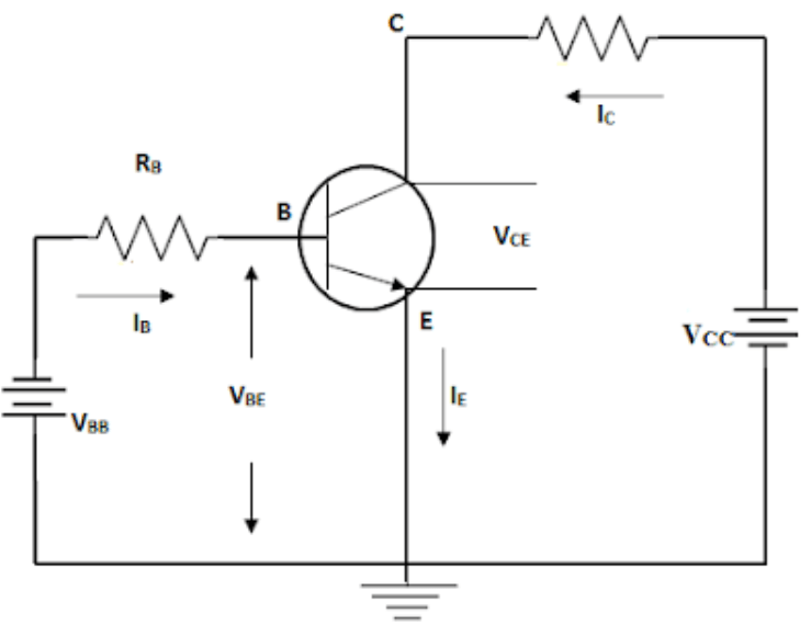
Figure 9: Common Emitter Configuration
Common Emitter (CE) Configuration
The common emitter configuration is the most popular due to its strong amplification properties, offering both significant current and voltage gain. The input is applied between the base and emitter, and the output is taken across the collector-emitter junction. This setup makes it versatile, and suitable for amplifying audio signals in consumer electronics and serving as the switching element in digital circuits. Its effective amplification and ability to drive loads make it widely used in various applications.
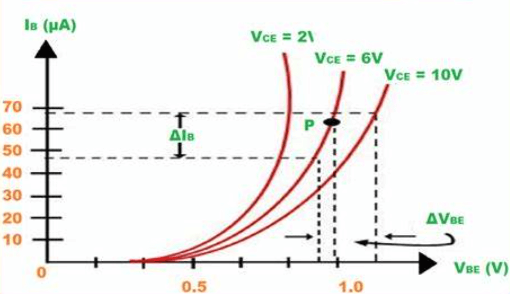
Figure 10: Common Emitter Input Characteristics
In the common emitter configuration, understanding the input circuit behavior is essential for grasping transistor operation. The process starts with the base-emitter voltage (VBE) at zero and increases gradually while keeping the collector-emitter voltage (VCE) at zero. Initially, the base current (IB) rises, showing a diode-like forward bias at the base-emitter junction. Graphs illustrate this with a steep increase in IB as VBE goes up, highlighting the junction's voltage sensitivity.
When VCE is set to a higher value, such as 10 volts, starting again from zero VBE, the input characteristics curve shifts noticeably. This shift occurs because the reverse bias at the collector-base junction widens the depletion region. As a result, a higher VBE is needed to achieve the same IB as before.
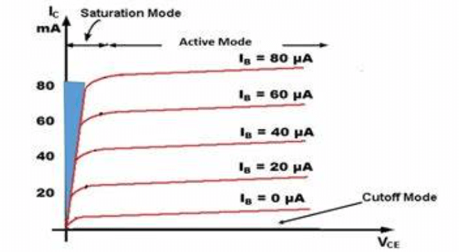
Figure 11: Common Emitter Output Characteristics
To study the output characteristics in a common emitter setup, set a fixed base current (IB), like 20 μA, and vary the collector-emitter voltage (VCE). This method maps the transistor's behavior from cut-off to saturation, showing a clear relationship between increasing VCE and the resulting collector current (IC)..
The saturation region is particularly important, where the transistor conducts efficiently. Here, both the emitter-base and collector-base junctions are forward-biased, causing a rapid rise in IC with small increases in VCE.
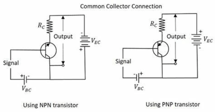
Figure 12: Common Collector Configuration
Common Collector (CC) Configuration
The common collector configuration, also known as the emitter follower, has high input impedance and low output impedance. The input signal is applied to the base, and the output is taken from the emitter, which closely follows the input voltage. This setup provides unity voltage gain, meaning the output voltage nearly matches the input voltage. It is primarily used for voltage buffering, making it useful for interfacing high-impedance sources with low-impedance loads, enhancing signal integrity without significant amplification.
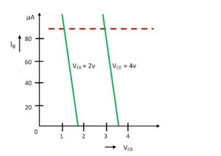
Figure 13: Common Collector Input Characteristics
The common collector configuration, known as the emitter follower because the output follows the input, has unique input characteristics. To study these, we vary the base-collector voltage (VBC) while keeping the output voltage (VEC) fixed, starting at 3 volts. As VBC increases from zero, the input current (IB) begins to rise, directly responding to changes in VBC. This relationship is shown graphically to depict how the transistor reacts to incremental input changes.
When VEC is increased to higher levels, we observe how the input characteristics shift, highlighting the transistor’s adaptation to higher output voltages. This information is crucial for understanding the high input resistance of the common collector configuration, which is advantageous for impedance-matching applications, minimizing signal loss between stages.
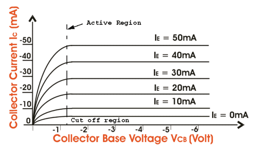
Figure 14: Common Collector Output Characteristics
To examine the output characteristics of the common collector configuration, we fix the input current and vary the output voltage (VEC). With no input current, the transistor remains non-conductive, in the cut-off region. As the input current increases, the transistor enters its active region, mapping the relationship between the emitter current (IE) and VEC. This mapping demonstrates the low output resistance of this configuration, beneficial for voltage buffering applications.
Pros and Cons of Using Bipolar Junction Transistors
Pros
BJTs are prized in electronics for their excellent amplification abilities. They are requisite in circuits needing significant boosts in voltage and current. These transistors provide high voltage gains and work effectively in various modes: active, reverse, saturation, and cutoff. Each mode has specific benefits, making BJTs versatile for different electronic applications. In active mode, a BJT can amplify weak signals without saturating, ideal for linear amplification tasks. They also handle high-frequency signals well, which is useful in RF (Radio Frequency) communication systems. Furthermore, BJTs can function as switches, making them suitable for a range of electronic components and systems, from simple signal switches to complex logic circuits.
Cons
However, BJTs have some drawbacks. They are prone to thermal instability, meaning temperature changes can affect their performance, causing inefficiencies or noise in the output. This is a significant issue in precision applications. Besides, compared to FETs, BJTs have slower switching speeds and consume more power, which is a disadvantage in modern electronics that require fast switching and energy efficiency. This slower response and higher power consumption limit their use in certain high-speed and power-sensitive applications, where FETs, with their quicker and more energy-efficient performance, might be more suitable.
Applications of Bipolar Junction Transistors in Modern Electronics
BJTs play an insistent role in many electronic circuits, especially in amplification and switching. They are required for circuits needing precise control over audio, current, and voltage amplification. In amplifier designs, NPN transistors are often preferred over PNP types because electrons, which are the charge carriers in NPN transistors, move faster and more efficiently than holes, the charge carriers in PNP transistors. This results in better amplification performance.
BJTs are used in a variety of applications, from small audio devices to large industrial machines. In audio amplification, they amplify tiny signals from microphones to levels suitable for speakers. In digital circuits, their ability to switch quickly allows them to act as binary switches, dangerous for logic operations in computers.
In addition, BJTs are needed in oscillators and modulators and are needed for signal generation and modification in telecommunications. Their rapid switching ability and capacity to handle varying power levels make them key components in producing frequency-based signals.
The Development of Bipolar Junction Transistors
Advances in semiconductor doping techniques were key to creating new BJT types, such as micro-alloy, micro-alloy diffused, and post-alloy transistors. These new variants showed significant improvements in speed and energy efficiency, meeting the increasing demand for faster and more reliable electronic components.
A breakthrough in BJT development was the introduction of the diffused transistor and the planar transistor. These innovations made the manufacturing process more efficient, enabling the integration of BJTs into smaller and more complex circuits. This progress paved the way for mass production of integrated circuits, which in turn drove rapid advancements in consumer electronics. Today, BJTs are found in a wide range of applications, from computing and communications to automation and control systems. Their continued presence in these fields highlights their lasting importance and adaptability in modern electronics.
Conclusion
Bipolar Junction Transistors (BJTs) are integral to modern electronics, providing robust solutions for amplification and switching across a spectrum of applications. Through the detailed examination of their design, operation, and the nuances of their functionality in various regions—active, saturation, and cut-off—BJTs demonstrate a remarkable flexibility and efficiency that is dynamic for both signal integrity and power management in electronic circuits.
Despite some limitations, such as thermal instability and relative inefficiency compared to Field Effect Transistors (FETs), BJTs continue to evolve with advancements in semiconductor technology, ensuring their relevance in the ever-evolving landscape of electronic design. Their enduring utility in amplifying weak signals, managing power efficiently, and switching rapidly between states underpins their obligatory role in both analog and digital electronics, from basic audio devices to sophisticated computational systems. The ongoing development and refinement of BJTs, marked by innovations like the planar and diffused transistor, underscore their serious contribution to the progress and reliability of contemporary electronic components and systems.
Frequently Asked Questions [FAQ]
1. What is a bipolar transistor explain its structure?
A bipolar transistor is a semiconductor device that consists of three layers of doped material, forming two p-n junctions. The three regions are called the emitter, base, and collector. The emitter is heavily doped to inject charge carriers (electrons or holes) into the base, which is very thin and lightly doped to allow easy passage of these carriers to the collector, which is moderately doped and designed to collect these carriers.
2. What are the characteristics of a bipolar transistor?
Bipolar transistors exhibit three key characteristics:
Amplification: They can amplify an input signal, providing a larger output.
Switching: They can act as switches, turning on (conducting) or off (non-conducting) based on the input signal.
Current Control: The current between the collector and emitter is controlled by the current flowing through the base.
3. What is the basic concept of bipolar transistor?
The ultimate concept behind a bipolar transistor is its ability to control and amplify current. It operates as a current-driven device, where a small current entering the base controls a larger current flowing from the collector to the emitter. This makes it an effective tool for amplifying signals in various electronic circuits.
4. What is the objective of a bipolar junction transistor?
The primary objective of a bipolar junction transistor is to function as a current amplifier. By leveraging small base currents to control larger collector-emitter currents, BJTs serve key roles in amplification and switching applications in electronic circuits.
5. What is the function of the base in a bipolar junction transistor?
The base of a bipolar junction transistor plays a serious role in controlling the transistor’s operation. It acts as a gatekeeper for the charge carriers. The current applied to the base regulates the number of carriers able to cross from the emitter to the collector, thus controlling the overall current flow through the transistor. This small base current manipulation allows the transistor to achieve signal amplification or act as an electronic switch.
About us
ALLELCO LIMITED
Read more
Quick inquiry
Please send an inquiry, we will respond immediately.
Low-Pass Filters Unveiled: A Comprehensive Guide to Their Function and Impact
on June 14th

Evaluating Power Factor in Electrical Circuits
on June 13th
Popular Posts
-
What is GND in the circuit?
on January 1th 2946
-

RJ-45 Connector Guide: RJ-45 Connector Color Codes, Wiring Schemes, R-J45 Applications, RJ-45 Datasheets
on January 1th 2502
-

Fiber Connector Types: SC Vs LC And LC Vs MTP
on January 1th 2091
-
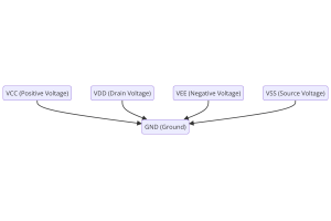
Understanding Power Supply Voltages in Electronics VCC, VDD, VEE, VSS, and GND
on November 9th 1898
-

Comparison Between DB9 and RS232
on January 1th 1765
-

What Is An LR44 Battery?
Electricity, that ubiquitous force, quietly permeates every aspect of our daily lives, from trivial gadgets to life-threatening medical equipment, it plays a silent role. However, truly grasping this energy, especially how to store and efficiently output it, is no easy task. It is against this background that this article will focus on a type of coin cell battery that may seem insignificant on the...on January 1th 1714
-
Understanding the Fundamentals:Inductance Resistance, andCapacitance
In the intricate dance of electrical engineering, a trio of fundamental elements takes center stage: inductance, resistance, and capacitance. Each bears unique traits that dictate the dynamic rhythms of electronic circuits. Here, we embark on a journey to decipher the complexities of these components, to uncover their distinct roles and practical uses within the vast electrical orchestra. Inductan...on January 1th 1662
-

CR2430 Battery Comprehensive Guide: Specifications, Applications and Comparison to CR2032 Batteries
What is CR2430 battery ?Benefits of CR2430 BatteriesNormCR2430 Battery ApplicationsCR2430 EquivalentCR2430 VS CR2032Battery CR2430 SizeWhat to look for when buying the CR2430 and equivalentsData Sheet PDFFrequently Asked Questions Batteries are the heart of small electronic devices. Among the many types available, coin cells play a crucial role, commonly found in calculators, remote controls, and ...on January 1th 1567
-
What Is RF and Why Do We Use It?
Radio Frequency (RF) technology is a key part of modern wireless communication, enabling data transmission over long distances without physical connections. This article delves into the basics of RF, explaining how electromagnetic radiation (EMR) makes RF communication possible. We will explore the principles of EMR, the creation and control of RF signals, and their wide-ranging uses. The article ...on January 1th 1550
-

CR2450 vs CR2032: Can The Battery Be Used Instead?
Lithium manganese batteries do have some similarities with other lithium batteries. High energy density and long service life are the characteristics they have in common. This kind of battery has won the trust and favor of many consumers because of its unique safety. Expensive tech gadgets? Small appliances in our homes? Look around and you'll see them everywhere. Among these many lithium-manganes...on January 1th 1519
HOT Part Number
-

ADP3335ACPZ-1.8-R7
Analog Devices Inc.
IC REG LINEAR 1.8V 500MA 8LFCSP
2CL71A
Diotec Semiconductor
DIODE GEN PURP 8KV 5MA AXIAL
AOD2N100M
Alpha & Omega Semiconductor Inc.
MOSFET N-CH TO252
DZ2S068C0L
Panasonic Electronic Components
TVS DIODE 4VWM SSMINI2-F5-B
12102C153JAT2A
KYOCERA AVX
CAP CER 0.015UF 200V X7R 1210
ADP7102ARDZ-1.5-R7
Analog Devices Inc.
IC REG LINEAR 1.5V 300MA 8SOIC
DG536DN
Vishay Siliconix
IC AMP/VIDEO/MUX LP 2CH 44PLCC
LMV934MT
Texas Instruments
IC OPAMP GP 4 CIRCUIT 14TSSOP
MA4P604-255
MACOM Technology Solutions
DIODE,PIN,CERAMIC_PKG,SI
TMP513AIRSAR
Texas Instruments
IC TEMP SNSR TRIPL REMOTE 16QFN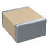
C1812C334K5RAC7800
KEMET
CAP CER 0.33UF 50V X7R 1812
MAX2169ETL+
Analog Devices Inc./Maxim Integrated
IC TUNER BROADBAND MOBILE 40TQFN
C0603X5R1C224K030BC
TDK Corporation
CAP CER 0.22UF 16V X5R 0201
MIC5841BN
Microchip Technology
IC PWR DRIVER BIPOLAR 1:8 18DIP
PI3A6386ZLEX
Diodes Incorporated
ANALOG SWITCH 3V-5V V-QFN3030-24
4816P-1-100LF
Bourns Inc.
RES ARRAY 8 RES 10 OHM 16SOIC
XC9260B33CPR-G
Torex Semiconductor Ltd
1.5A COT CONTROL SYNCHRONOUS STE
PEX8625-AA50RBC F
Broadcom Limited
PEX8625-AA50RBC F -
F921V224MAA
KYOCERA AVX
CAP TANT 0.22UF 20% 35V 1206
MMZ1608S301CTAH0
TDK Corporation
FERRITE BEAD 300 OHM 0603 1LN
SCN-2-19+
Mini-Circuits
RF PWR DVDR 1.425GHZ-1.9GHZ 6SMD
GRM1886S1H240JZ01D
Murata Electronics
CAP CER 24PF 50V S2H 0603
TAJD336K025RNJ
KYOCERA AVX
CAP TANT 33UF 10% 25V 2917
DS80C310-QCG+
Analog Devices Inc./Maxim Integrated
IC MCU 8BIT ROMLESS 44PLCC
08051U151KAT2A
KYOCERA AVX
CAP CER 150PF 100V NP0 0805
AWB7228P8
Skyworks Solutions Inc.
IC AMP HSDPA 2.496-2.69GHZ 14SMD
TSL2550T
ams OSRAM
SENSOR OPT 640NM AMBIENT 4SMD
CM1406-04DE
onsemi
FILTER RC(PI) 200 OHM/15PF SMD
4816P-2-332
Bourns Inc.
RNET-THK FILM SMD MED BODY
RJK03J9DNS-00#J5
Renesas Electronics America Inc
N-CHANNEL POWER SWITCHING MOSFET
GRM1555C1E4R2BZ01D
Murata Electronics
CAP CER 4.2PF 25V C0G/NP0 0402
DZ2736000L
Panasonic Electronic Components
DIODE ZENER 36V 120MW SSSMINI2
GA243DR7E2472MW01L
Murata Electronics
CAP CER 4700PF 250VAC X7R 1812
DF3-2428SCF
Hirose Electric Co Ltd
CONN SOCKET 24-28AWG CRIMP TIN
IXGT60N60B2
IXYS
IGBT 600V 75A 500W TO268
D82C284-12
Intel
CLOCK GENERATOR -
MB85RS1MTPNF-G-JNERE1
Kaga FEI America, Inc.
IC FRAM 1MBIT SPI 40MHZ 8SOP
LTC4252-1IMS#PBF
Analog Devices Inc.
IC HOT SWAP CTRLR -48V 10MSOP
STP120NF04
STMicroelectronics
MOSFET N-CH 40V 120A TO220AB
1N5246B
onsemi
DIODE ZENER 16V 500MW DO35
MIC69502WR-TR
Microchip Technology
IC REG LINEAR POS ADJ 5A SPAK-7
MM74HC04MX
onsemi
IC INVERTER 6CH 1-INP 14SOIC
ESDA7P60-1U1M
STMicroelectronics
TVS DIODE 5VWM 11.6VC 1610
T520D227M006ATE009
KEMET
CAP TANT POLY 220UF 6.3V 2917
CAT24C04HU4I-GT3
onsemi
IC EEPROM 4KBIT I2C 400KHZ 8UDFN
STH160N4LF6-2
STMicroelectronics
MOSFET N-CH 40V 120A H2PAK-2
RT0805DRE0724R9L
YAGEO
RES SMD 24.9 OHM 0.5% 1/8W 0805
NCP81075DR2G
onsemi
IC GATE DRVR HI/LOW SIDE 8SOIC
MPS6534
Fairchild Semiconductor
TRANS PNP 40V 0.8A TO92-3
SI9410BDY-T1-E3
Vishay Siliconix
MOSFET N-CH 30V 6.2A 8SO
SMBJ17CA-E3/52
Vishay General Semiconductor - Diodes Division
TVS DIODE 17VWM 27.6VC DO214AA
MAX3238EAI
Analog Devices Inc./Maxim Integrated
IC TRANSCEIVER FULL 5/3 28SSOP
MIC2920A-5.0BT
Microchip Technology
IC REG LINEAR 5V 400MA TO220-3
P4SMA47AHE3/5A
Vishay General Semiconductor - Diodes Division
TVS DIODE 40.2VWM 64.8VC DO214AC