2N3906 Transistor Comprehensive Guide-Pin Configurations, Application Scenarios and Equivalents, and How to Test
Catalog
Brief Overview of the 2N3906
Features and Technical Specifications of 2N3906
- - Complementary to the 2N3904/MMBT3904 bipolar transistors
- - Collector-Emitter Voltage (VCE): 40V
- - Emitter-Base Voltage (VBE): 5V
- - Continuous Collector Current (IC): 200mA
- - Operating temperature range: -55 to 150°C
- - Base Current (IB): Maximum 5mA
- - DC Current Gain (hFE): 60
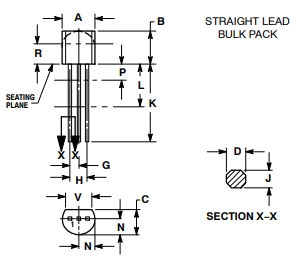
- - Enclosed in a To-92 package
- - Collector-Base Voltage (VCB): 40V
- - Lead-free package options available
- - Collector-Emitter Saturation Voltage: 0.25V
- - Maximum Power Dissipation: 250mW
Pin Configuration and Schematic of the 2N3906
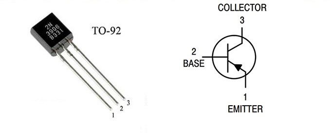
|
Pin Number |
Pin Name |
Description |
|
1 |
Emitter |
Current Drains out through the emitter |
|
2 |
Base |
Controls the biasing of transistor |
|
3 |
Collector |
Current flows in through the collector |
Applications of the 2N3906
Common application scenarios for the 2N3906 transistor include:
- - High to low current load switching
- - Inverters and converter circuits
- - Darlington pair circuits
- - Alarm systems or dual LED setups
- - Low-power amplification circuits
- - Flash units
- - High-speed switching applications
- - General-purpose audio amplifiers
- - Suitable for loads with peak voltages up to 40V
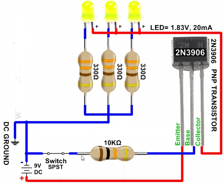
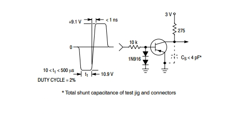
Circuit for 2N3906
An example is a switch
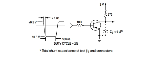
2N3906 Delay and Rise Time Test Circuitry
2N3906 Storage and Falling Time Equivalent Test Circuit
How to Test the 2N3906
Before starting to test the 2N3906 transistor, ensure you have the following tools:
- - Multimeter
- - DC power source
- - Resistors with known resistance values
- - Connecting wires
The testing process for the 2N3906 transistor involves several steps:
Safety Tips When Using Transistors:
- - Avoid operating transistors under conditions exceeding 20V or 700mA to prevent damage.
- - Use base resistors of appropriate values to keep the base current within safe limits specified in datasheets or reference materials.
- - Do not expose transistors to temperatures above 150°C to avoid thermal damage.
2N3906 vs. BC557
High Collector-Emitter Voltage:
Gain Value:
Application Limitations:
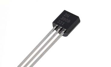
2N3906 Package
Download Datasheet
Frequently Asked Questions [FAQ]
1. What is the difference between 2N3904 and 2N3906?
2. What is the maximum base current of 2N3906?
3. What is the difference between PNP and NPN?
About us
ALLELCO LIMITED
Read more
Quick inquiry
Please send an inquiry, we will respond immediately.
CR3032 – The First Choice for Equipment with Higher Energy Demands
on April 16th
What is SMD Packaging?
on April 12th
Popular Posts
-
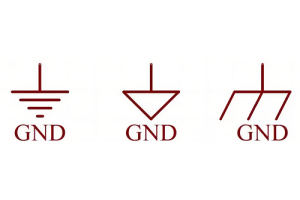
What is GND in the circuit?
on January 1th 3272
-

RJ-45 Connector Guide: RJ-45 Connector Color Codes, Wiring Schemes, R-J45 Applications, RJ-45 Datasheets
on January 1th 2815
-
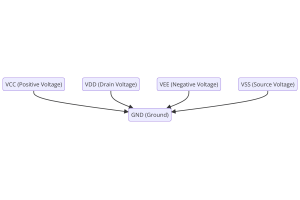
Understanding Power Supply Voltages in Electronics VCC, VDD, VEE, VSS, and GND
on November 20th 2642
-

Fiber Connector Types: SC Vs LC And LC Vs MTP
on January 1th 2265
-

Comparison Between DB9 and RS232
on January 1th 1882
-

What Is An LR44 Battery?
Electricity, that ubiquitous force, quietly permeates every aspect of our daily lives, from trivial gadgets to life-threatening medical equipment, it plays a silent role. However, truly grasping this energy, especially how to store and efficiently output it, is no easy task. It is against this background that this article will focus on a type of coin cell battery that may seem insignificant on the...on January 1th 1846
-
Understanding the Fundamentals:Inductance Resistance, andCapacitance
In the intricate dance of electrical engineering, a trio of fundamental elements takes center stage: inductance, resistance, and capacitance. Each bears unique traits that dictate the dynamic rhythms of electronic circuits. Here, we embark on a journey to decipher the complexities of these components, to uncover their distinct roles and practical uses within the vast electrical orchestra. Inductan...on January 1th 1808
-
What Is RF and Why Do We Use It?
Radio Frequency (RF) technology is a key part of modern wireless communication, enabling data transmission over long distances without physical connections. This article delves into the basics of RF, explaining how electromagnetic radiation (EMR) makes RF communication possible. We will explore the principles of EMR, the creation and control of RF signals, and their wide-ranging uses. The article ...on January 1th 1801
-
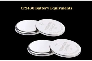
CR2430 Battery Comprehensive Guide: Specifications, Applications and Comparison to CR2032 Batteries
What is CR2430 battery ?Benefits of CR2430 BatteriesNormCR2430 Battery ApplicationsCR2430 EquivalentCR2430 VS CR2032Battery CR2430 SizeWhat to look for when buying the CR2430 and equivalentsData Sheet PDFFrequently Asked Questions Batteries are the heart of small electronic devices. Among the many types available, coin cells play a crucial role, commonly found in calculators, remote controls, and ...on January 1th 1799
-
Comprehensive guide to hFE in transistors
Transistors are crucial components in modern electronic devices, enabling signal amplification and control. This article delves into the knowledge surrounding hFE, including how to select a transistor's hFE value, how to find hFE, and the gain of different types of transistors. Through our exploration of hFE, we gain a deeper understanding of how transistors work and their role in electronic circu...on November 20th 1782
HOT Part Number
-

EPM7064STC44-5
Intel
IC CPLD 64MC 5NS 44TQFP
X5163S8-2.7
Renesas Electronics America Inc
IC SUPERVISOR 1 CHANNEL 8SOIC
SP6205ER-L
MaxLinear, Inc.
IC REG LINEAR POS ADJ 500MA 8DFN
GRM31A5C2H391JW01D
Murata Electronics
CAP CER 390PF 500V C0G/NP0 1206
PIC16LF18313-I/RF
Microchip Technology
IC MCU 8BIT 3.5KB FLASH 8UDFN
40CPQ100
Vishay General Semiconductor - Diodes Division
DIODE ARRAY SCHOTTKY 100V TO247
2N6517TA
onsemi
TRANS NPN 350V 0.5A TO92-3
10CL010YE144I7G
Intel
IC FPGA 88 I/O 144EQFP
SNJ54S195J
Texas Instruments
PARALLEL IN PARALLEL OUT
UMK105SL121JV-F
Taiyo Yuden
CAP CER 120PF 50V SL/GP 0402
BAS19W
Taiwan Semiconductor Corporation
SOT-323, 100V, 0.2A, SWITCHING D
MIC69502WU
Micrel Inc.
5 AMP, LOW VIN, LOW VOUT MICRO C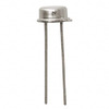
LM185BYH-2.5
Texas Instruments
IC VREF SHUNT 1.5% TO2
SMBJ48CA-E3/5B
Vishay General Semiconductor - Diodes Division
TVS DIODE 48VWM 77.4VC DO214AA
CL10C221KD8NNNC
Samsung Electro-Mechanics
CAP CER 220PF 200V C0G/NP0 0603
ICL7106CM44
Renesas Electronics America Inc
IC DISPLAY DRVR 3.5DIGIT 44MQFP
IRFS3806TRLPBF
Infineon Technologies
MOSFET N-CH 60V 43A D2PAK
ISO7760FDBQR
Texas Instruments
DGTL ISO 3000VRMS 6CH GP 16SSOP -
NPPN031BFLC-RC
Sullins Connector Solutions
CONN HDR 3POS 0.079 GOLD SMD
IR2233JPBF
Infineon Technologies
IC GATE DRVR HALF-BRIDGE 44PLCC
LDS6202NTGI
Renesas Electronics America Inc
IC TOUCH CTLR 4CH CAP 16VFQFPN
DS620U+
Analog Devices Inc./Maxim Integrated
SENSOR DIGITAL -55C-125C 8UMAX
RGPR30BM40HRTL
Rohm Semiconductor
IGBT 430V 30A IGNITION TO252
MPC8250AZUMHBC
NXP USA Inc.
IC MPU MPC82XX 266MHZ 480TBGA
EMC2113-1-AP-TR
Microchip Technology
IC RPM FAN CTRLR 16QFN
UC2902N
Texas Instruments
IC LOAD SHARE CONTROLLER 8DIP
2SD1781KT146Q
Rohm Semiconductor
TRANS NPN 32V 0.8A SMT3
EPC1441LI20N
Intel
IC CONFIG DEVICE 20PLCC
LT1714IGN#TRPBF
Analog Devices Inc.
IC COMPARATOR 2 W/LATCH 16SSOP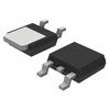
NID6002NT4G
onsemi
IC PWR DRIVER N-CHANNEL 1:1 DPAK
AD9954YSVZ-REEL7
Analog Devices Inc.
IC DDS 400MHZ 14BIT 48TQFP
S-5844A85CD-A4T2U3
ABLIC Inc.
THERMOSTAT OPEN DRAIN HSNT4-B
TLV2460IP
Texas Instruments
IC OPAMP GP 1 CIRCUIT 8DIP
AT45DB321E-MWHF-T
Adesto Technologies
IC FLASH 32MBIT SPI 85MHZ 8VDFN
PIC12LF1501-E/MF
Microchip Technology
IC MCU 8BIT 1.75KB FLASH 8DFN
ISL88031IU8HEZ-TK
Renesas Electronics America Inc
IC SUPERVISOR 5 CHANNEL 8MSOP -
R5F100MHAFA#V0
Renesas Electronics America Inc
IC MCU 16BIT 192KB FLASH 80LQFP
C430N
Powerex Inc.
SCR 800V 1070A PRESS-PAK
C3216JB2J332K115AA
TDK Corporation
CAP CER 3300PF 630V JB 1206
NCP600SN350T1G
onsemi
IC REG LINEAR 3.5V 150MA 5TSOP
M74VHC1GT04DTT1G
onsemi
IC INVERTER 1CH 1-INP 5TSOP
HX5084NL
Pulse Electronics
MODULE 4CH EXTEMP GIGABIT 24SOIC
UC2845AQD8
Texas Instruments
IC REG CTRLR MULT TOPOLOGY 8SOIC
GCM1885C2A2R8CA16D
Murata Electronics
CAP CER 2.8PF 100V C0G/NP0 0603
INA190A3IRSWT
Texas Instruments
IC CURR SENSE 1 CIRCUIT 10UQFN
VLS252010HBX-6R8M-1
TDK Corporation
FIXED IND 6.8UH 1.1A 406MOHM SMD
VBO88-12NO7
IXYS
BRIDGE RECT 1P 1.2KV 92A ECOPAC2
MIMXRT685SFVKB
NXP USA Inc.
IC MCU 32BIT EXT MEM 176VFBGA
CD54ACT08F3A
Texas Instruments
CD54ACT08 QUAD 2-INPUT AND GATES
MCP6284-E/ST
Microchip Technology
IC OPAMP GP 4 CIRCUIT 14TSSOP
TPS536C7B1RSLR
Texas Instruments
IC POWER
9DBL0253ANLGI8
Renesas Electronics America Inc
9DBL0253A 2-O/P LP-HCSL ZDB, ZO=
BQ24210DQCR
Texas Instruments
IC BATT CHG LI-ION 1CELL 10WSON
GRM1885C1H470JA01D
Murata Electronics
CAP CER 47PF 50V C0G/NP0 0603