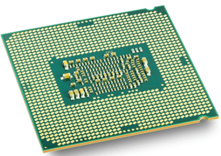
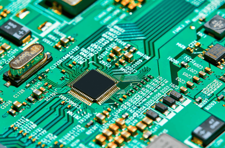
What is SMD Packaging?
Catalog
Introduction to SMD Packaging
|
SMD Package Size |
Length (mm) |
Width (mm) |
Height (mm) |
|
0201 |
0.6 |
0.3 |
0.3 |
|
0402 |
1.0 |
0.5 |
0.35 |
|
0603 |
1.6 |
0.8 |
0.35 |
|
0805 |
2.0 |
1.25 |
0.45 |
|
1206 |
3.2 |
1.6 |
0.45 |
|
1210 |
3.2 |
2.5 |
0.45 |
|
1812 |
4.5 |
3.2 |
0.45 |
|
2010 |
5.0 |
2.5 |
0.45 |
|
2512 |
6.4 |
3.2 |
0.45 |
|
5050 |
5.0 |
5.0 |
0.8 |
|
5060 |
5.0 |
6.0 |
0.8 |
|
5630 |
5.6 |
3.0 |
0.8 |
|
5730 |
5.7 |
3.0 |
0.8 |
|
7030 |
7.0 |
3.0 |
0.8 |
|
7070 |
7.0 |
7.0 |
0.8 |
|
8050 |
8.0 |
5.0 |
0.8 |
|
8060 |
8.0 |
6.0 |
0.8 |
|
8850 |
8.0 |
5.0 |
0.8 |
|
3528 |
8.9 |
6.4 |
0.5 |
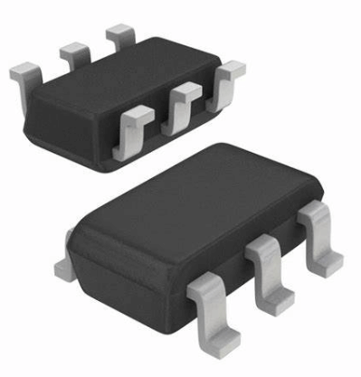
Types of SMD Packaging and Their Applications
|
Chip package type |
Dimensions in mm |
Dimensions in inches |
|
01005 |
0.4x0.2 |
0.016x0.008 |
|
015015 |
0.38 x 0.38 |
0.014x0.014 |
|
0201 |
0.6x03 |
0.02x 0.01 |
|
0202 |
0.5x0.5 |
0.019 x0.019 |
|
02404 |
0.6 x1.0 |
0.02 x0.03 |
|
0303 |
0.8x0.8 |
0.03x0.03 |
|
0402 |
1.0x0.5 |
0.04x0.02 |
|
0603 |
1.5 x 0.8 |
0.06 x 0.03 |
|
0805 |
2.0x1.3 |
0.08x0.05 |
|
1008 |
2.5x2.0 |
0.10x0.08 |
|
1777 |
2.8x2.8 |
0.11 x 0.11 |
|
1206 |
3.0 x1.5 |
0.12 x0.06 |
|
1210 |
3.2x2.5 |
0.125 x0.10 |
|
1806 |
4.5x1.6 |
0.18x0.06 |
|
1808 |
4.5x2.0 |
0.18 x0.07 |
|
1812 |
4.6x3.0 |
0.18 x 0.125 |
|
1825 |
4.5x6.4 |
0.18 x0.25 |
|
2010 |
5.0x2.5 |
0.20x0.10 |
|
2512 |
6.3x3.2 |
0.25 x0.125 |
|
2725 |
6.9 x 6.3 |
0.27 x0.25 |
|
2920 |
7.4x5.1 |
0.29 x0.20 |
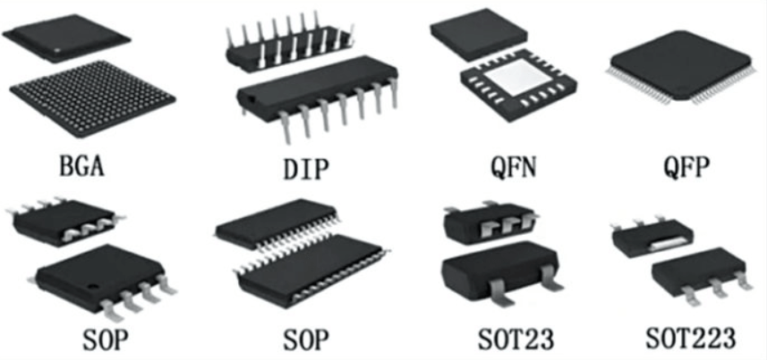
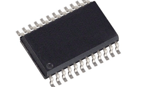
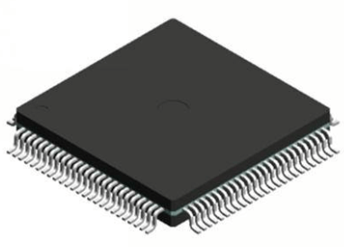
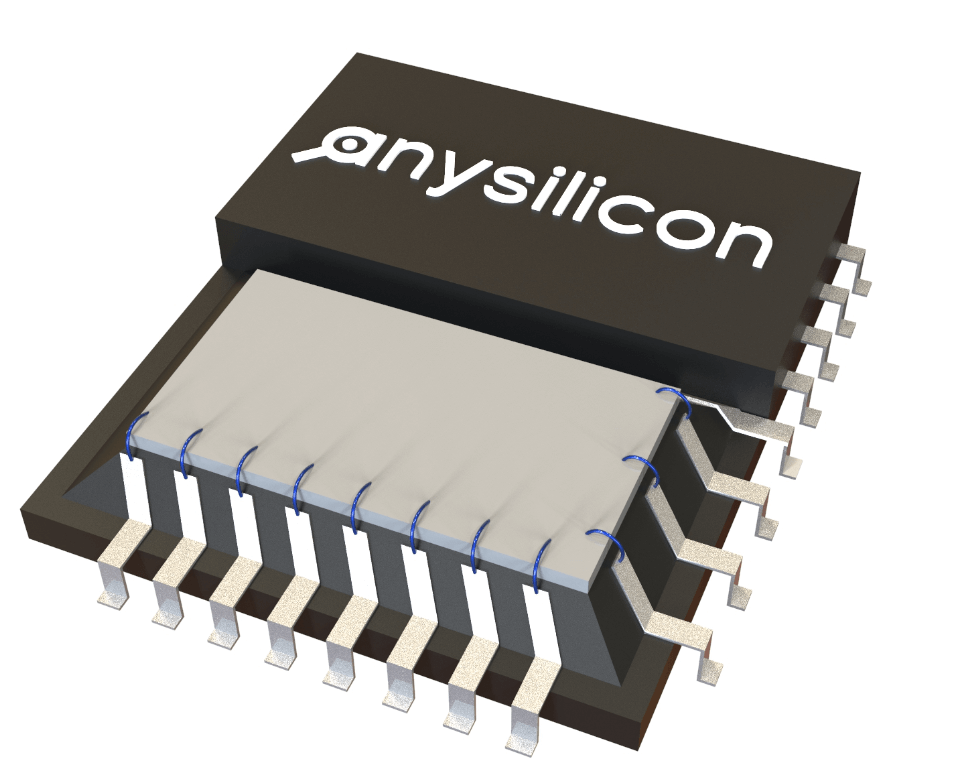
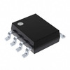
Types of SMD Integrated Circuit Packaging
|
Package type |
Properties |
Application |
|
SOIC |
1. Small outline integrated circuit 2. Surface-mount equivalent of the classic through-hole DiP (Dual-inline Package) |
1. Standard package for logic lC |
|
TSSOP |
1. Thin shrink small outline package 2. Rectangular surface mount 3. Plastic integrated circuit (lC) package 4. Gull-wing leads |
1. Analog amplifiers, 2. Controllers and Drivers 3. Logic devices 4. Memory devices 5. RF/wireless 6. Disk drives |
|
QFP |
1. Quad flat package. 2. Easiest option for high pin-count components 3. Easy to inspect by AOl 4. Assembled with standard reflow soldering |
1. Microcontrollers 2. Multi-channel codecs
|
|
QFN |
1. Quad flat no-lead 2. Electrical contacts do not come out of the component 3. Smaller than QFP 4. Require extra attention in PCB assembly |
1. Microcontrollers. 2. Multi-channel codecs |
|
PLCC |
1. Ball grid array 2. Most complex 3. High-pin count component 4. Electrical components are below silicon lC 5. Requires reflow soldering for PCB assembly |
1. Prototype PCB assembly
|
|
BCA |
1. Plastic leaded chip carrier 2. Allow components to be directly mounted on the PCB |
1. High-speed microprocessor 2. Field programming gate array(FPGA) |
|
POP |
1. Package-on package technology 2. Stacked on the top of others |
1. Used for memory devices and microprocessors 2. High-speed design, HDL design |
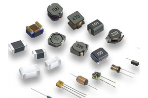
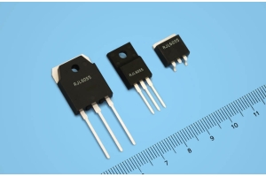
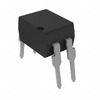
SMD Resistor Packaging Sizes
Characteristics of Surface-Mount Devices (SMD)
|
Packages |
Dimensions(mm) |
Applications |
Component type |
Number of pins |
|
SMA |
3.56 x2.92 |
RF and microwave devices |
Diode |
2 |
|
D0-214 |
5.30x6.10 |
Power rectification diodes |
Diode |
2 |
|
DO-213AA |
4.57 x3.94 |
Small signal transistors and diodes |
Diode |
2 |
|
SMC |
5.94x5.41 |
Integrated circuits, resistors, and capacitors Power MOSFETs and voltage regulators |
Diode |
2 |
|
TO-277 |
3.85 x3.85 |
Power MOSFETs and voltage regulators |
MOSFET |
3 |
|
MBS |
2.60 x1.90 |
Switching diodes and high-density integrated circuits |
Diode |
2 |
|
S0D-123 |
2.60 x1.90 |
Small signal diodes and transistors |
Diode |
2 |
|
0603 |
1.6x0.8 |
Consumer, automotive, and industrial equipment |
Resistors, capacitors, and inductors |
2 |
|
0805 |
2.0 x1.25 |
Consumer, automotive, and industrial equipment |
Resistors, capacitors, and inductors |
2 |
|
1206 |
3.2 x1.6 |
Consumer, automotive, and industrial equipment |
Resistors, capacitors, and inductors |
2 |
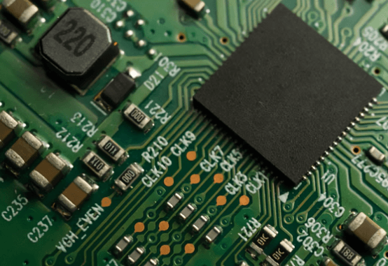
The Relationship Between SMD and SMT in Electronic Manufacturing
Conclusion
Frequently Asked Questions [FAQ]
1. What is an SMD package?
2. Why is SMD used?
3. What is the difference between SMD and SMT?
4. What are the types of SMD IC packages?
5. Are SMD components cheaper?
About us
ALLELCO LIMITED
Read more
Quick inquiry
Please send an inquiry, we will respond immediately.
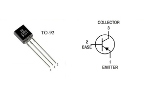
2N3906 Transistor Comprehensive Guide-Pin Configurations, Application Scenarios and Equivalents, and How to Test
on April 13th
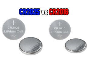
CR2025 VS CR2016: Which One Could Be Your First Choice?
on April 11th
Popular Posts
-
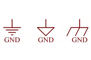
What is GND in the circuit?
on January 1th 3254
-

RJ-45 Connector Guide: RJ-45 Connector Color Codes, Wiring Schemes, R-J45 Applications, RJ-45 Datasheets
on January 1th 2803
-
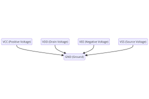
Understanding Power Supply Voltages in Electronics VCC, VDD, VEE, VSS, and GND
on November 20th 2610
-

Fiber Connector Types: SC Vs LC And LC Vs MTP
on January 1th 2250
-

Comparison Between DB9 and RS232
on January 1th 1867
-

What Is An LR44 Battery?
Electricity, that ubiquitous force, quietly permeates every aspect of our daily lives, from trivial gadgets to life-threatening medical equipment, it plays a silent role. However, truly grasping this energy, especially how to store and efficiently output it, is no easy task. It is against this background that this article will focus on a type of coin cell battery that may seem insignificant on the...on January 1th 1836
-
Understanding the Fundamentals:Inductance Resistance, andCapacitance
In the intricate dance of electrical engineering, a trio of fundamental elements takes center stage: inductance, resistance, and capacitance. Each bears unique traits that dictate the dynamic rhythms of electronic circuits. Here, we embark on a journey to decipher the complexities of these components, to uncover their distinct roles and practical uses within the vast electrical orchestra. Inductan...on January 1th 1791
-
What Is RF and Why Do We Use It?
Radio Frequency (RF) technology is a key part of modern wireless communication, enabling data transmission over long distances without physical connections. This article delves into the basics of RF, explaining how electromagnetic radiation (EMR) makes RF communication possible. We will explore the principles of EMR, the creation and control of RF signals, and their wide-ranging uses. The article ...on January 1th 1780
-
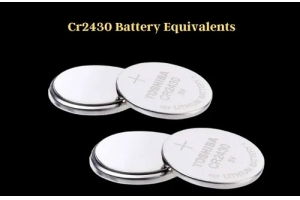
CR2430 Battery Comprehensive Guide: Specifications, Applications and Comparison to CR2032 Batteries
What is CR2430 battery ?Benefits of CR2430 BatteriesNormCR2430 Battery ApplicationsCR2430 EquivalentCR2430 VS CR2032Battery CR2430 SizeWhat to look for when buying the CR2430 and equivalentsData Sheet PDFFrequently Asked Questions Batteries are the heart of small electronic devices. Among the many types available, coin cells play a crucial role, commonly found in calculators, remote controls, and ...on January 1th 1775
-
Comprehensive guide to hFE in transistors
Transistors are crucial components in modern electronic devices, enabling signal amplification and control. This article delves into the knowledge surrounding hFE, including how to select a transistor's hFE value, how to find hFE, and the gain of different types of transistors. Through our exploration of hFE, we gain a deeper understanding of how transistors work and their role in electronic circu...on November 20th 1763
HOT Part Number
-
MAX6126AASA30+T
Analog Devices Inc./Maxim Integrated
IC VREF SERIES 0.02% 8SOIC
PTH05060WAST
Artesyn Embedded Power
DC DC CONVERTER 0.8-3.6V 36W
MAX7414CPA
Analog Devices Inc./Maxim Integrated
SWITCHED CAPACITOR FILTER
111MT80KB
Vishay General Semiconductor - Diodes Division
BRIDGE RECT 3PHASE 800V 110A MTK
V300C48T150B3
Vicor Corporation
DC DC CONVERTER 48V 150W
1812CC104MAT1A\SB
KYOCERA AVX
CAP CER 0.1UF 630V X7R 1812
BCM5482SA2KFB
Broadcom Limited
DUAL PORT 10/100/1000BASE-T PH
RC0402JR-07220RL
Yageo
RES SMD 220 OHM 5% 1/16W 0402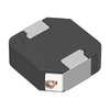
SPM10040T-220M-HZ
TDK Corporation
FIXED IND 22UH 5.2A 78.94MOHM SM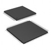
PIC24HJ256GP610-I/PT
Microchip Technology
IC MCU 16BIT 256KB FLASH 100TQFP
ISL62883CHRTZ-T
Renesas Electronics America Inc
IC REG CTRL IMVP-6.5 1OUT 40TQFN
170M5312
Eaton - Bussmann Electrical Division
FUSE SQUARE 630A 700VAC RECT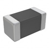
MMZ1608R300ATD25
TDK Corporation
FERRITE BEAD 30 OHM 0603 1LN
AD9460BSVZ-105
Analog Devices Inc.
IC ADC 16BIT PIPELINED 100TQFP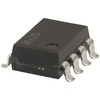
AQW224NAZ
Panasonic Electric Works
SSR RELAY SPST-NO 40MA 0-400V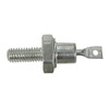
1N3892A
Solid State Inc.
12 AMP FAST RECOVERY RECTIFIER D
CSD17483F4
Texas Instruments
MOSFET N-CH 30V 1.5A 3PICOSTAR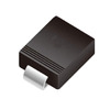
SMCJ40CA
MDD
TVS DIODE 40VWM 64.5VC SMC -
MMZ1608A222BTA00
TDK Corporation
FERRITE BEAD 2.2K OHM 0603 1LN
HI3-5043-5
Harris Corporation
IC SWITCH SPDT X 2 75OHM 16DIP
VI-B3L-CW
Vicor Corporation
DC DC CONVERTER 28V 100W
MAX172ACNG+
Analog Devices Inc./Maxim Integrated
IC ADC 12BIT CMOS 24-DIP
LM1117SX-ADJ
Texas Instruments
IC REG LIN POS ADJ 800MA DDPAK
QS6M4TR
Rohm Semiconductor
MOSFET N/P-CH 30V/20V 1.5A TSMT6
CA3227E
Intersil
NPN TRANSISTOR ARRAY
C2012X7T2W103M085AE
TDK Corporation
CAP CER 10000PF 450V X7T 0805
LM5176QPWPRQ1
Texas Instruments
IC POWER REGULATOR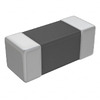
MMZ2012S181AT000
TDK Corporation
FERRITE BEAD 180 OHM 0805 1LN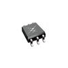
SI8710CD-B-IS
Skyworks Solutions Inc.
DGTL ISO 5000VRMS 1CH GP 6DIP GW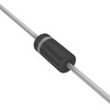
SA17ARLG
Littelfuse Inc.
TVS DIODE 17VWM 27.6VC AXIAL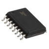
SP3232EBCT-L/TR
MaxLinear, Inc.
IC TRANSCEIVER FULL 2/2 16SOIC
MTM761230LBF
Panasonic Electronic Components
MOSFET P-CH 20V 3A WSMINI6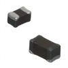
CBMF1608T100K
Taiyo Yuden
FIXED IND 10UH 380MA 468MOHM SMD
ISL5861IAZ
Renesas Electronics America Inc
IC DAC 12BIT A-OUT 28TSSOP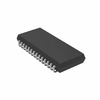
AS7C256A-15JCN
Alliance Memory, Inc.
IC SRAM 256KBIT PARALLEL 28SOJ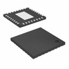
CY8C21434-24LCXI
Infineon Technologies
IC MCU 8BIT 8KB FLASH 32QFN -
TCET1100
Vishay Semiconductor Opto Division
OPTOISOLATR 5KV TRANSISTOR 4-DIP
RT8008GB
Richtek USA Inc.
IC REG BUCK ADJ 600MA SOT23-5
1N4553B
Solid State Inc.
DIODE ZENER 5.6V 50W DO5
1N2995RB
Microchip Technology
DIODE ZENER 47V 10W DO213AA
LTC4227CUFD-4#TRPBF
Analog Devices Inc.
IC HOT SWAP CTRLR GP 20QFN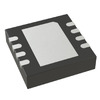
LTC4058EDD-4.2#TRPBF
Analog Devices Inc.
IC BATT CHG LI-ION 1CELL 8DFN
NJU7043V-TE1
Nisshinbo Micro Devices Inc.
IC CMOS 2 CIRCUIT 8SSOP
HA2-5177/883
Harris Corporation
IC OPAMP GP 1 CIRCUIT TO99-8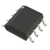
ADUM1281ARZ-RL7
Analog Devices Inc.
DGTL ISO 3000VRMS 2CH GP 8SOIC
RT0603BRE077R5L
YAGEO
RES SMD 7.5 OHM 0.1% 1/10W 0603
DAC161S997EVM
Texas Instruments
EVM MODULE FOR DAC161S997
C2012SL1A333J
TDK Corporation
CAP CER 0.033UF 10V SL 0805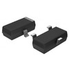
MLX90290LSE-AAA-511-RE
Melexis Technologies NV
SENSOR HALL EFFECT ANALOG TSOT3
UCC3919PW
Texas Instruments
IC HOT SWAP CTRLR GP 16TSSOP
SN2904DR
Texas Instruments
PROTOTYPE
JMK212AB7106MGHT
Taiyo Yuden
CAP CER 10UF 6.3V X7R 0805
ISL6308AIRZ-TS2705
Renesas Electronics America Inc
IC AMP CLASS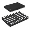
MP86885GQWT-P
Monolithic Power Systems Inc.
IC HALF BRIDGE DRIVER 40A 29TQFN