View All

Please refer to the English Version as our Official Version.Return

Europe
France(Français) Germany(Deutsch) Italy(Italia) Russian(русский) Poland(polski) Netherlands(Nederland) Spain(español) Turkey(Türk dili) Israel(עִבְרִית) Denmark(Dansk) Switzerland(Deutsch) United Kingdom(English)
Asia/Pacific
Japan(日本語) Korea(한국의) Thailand(ภาษาไทย) Malaysia(Melayu) Singapore(Melayu) Philippines(Pilipino)
Africa, India and Middle East
India(हिंदी)
North America
United States(English) Canada(English) Mexico(español)
HomeProductsDiscrete Semiconductor ProductsTransistors - FETs, MOSFETs - ArraysNTHC5513T1G
NTHC5513T1G Image
Image may be representation.
See specifications for product details.

NTHC5513T1G - onsemi

Manufacturer Part Number
NTHC5513T1G
Manufacturer
onsemi
Allelco Part Number
32D-NTHC5513T1G
ECAD Model
Parts Description
MOSFET N/P-CH 20V CHIPFET
Detailed Description
Package
8-SMD, Flat Lead
Data sheet
NTHC5513.pdf
RoHs Status
ROHS3 Compliant
In stock: 63990

Required fields are indicated by an asterisk (*)
Please send RFQ, we will respond immediately.

Quantity

Specifications

NTHC5513T1G Tech Specifications
onsemi - NTHC5513T1G technical specifications, attributes, parameters and parts with similar specifications to onsemi - NTHC5513T1G

Product Attribute Attribute Value  
Manufacturer onsemi  
Vgs(th) (Max) @ Id 1.2V @ 250µA  
Technology MOSFET (Metal Oxide)  
Supplier Device Package ChipFET™  
Series -  
Rds On (Max) @ Id, Vgs 80mOhm @ 2.9A, 4.5V  
Power - Max 1.1W  
Package / Case 8-SMD, Flat Lead  
Package Tape & Reel (TR)  
Product Attribute Attribute Value  
Operating Temperature -55°C ~ 150°C (TJ)  
Mounting Type Surface Mount  
Input Capacitance (Ciss) (Max) @ Vds 180pF @ 10V  
Gate Charge (Qg) (Max) @ Vgs 4nC @ 4.5V  
FET Feature Logic Level Gate  
Drain to Source Voltage (Vdss) 20V  
Current - Continuous Drain (Id) @ 25°C 2.9A, 2.2A  
Configuration N and P-Channel  
Base Product Number NTHC5513  

Parts Introduction

Manufacturer Part Number

NTHC5513T1G

Manufacturer

onsemi

Introduction

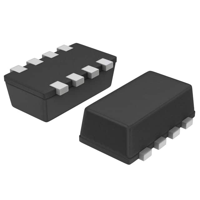
N-Channel and P-Channel MOSFET Array in ChipFET Package

Product Features and Performance

-55°C to 150°C Operating Temperature Range

1W Max Power Dissipation

20V Drain-to-Source Voltage

80mOhm Maximum On-Resistance

9A/2.2A Continuous Drain Current

180pF Input Capacitance

Logic Level Gate

Product Advantages

Compact ChipFET package

Wide temperature range

Low on-resistance

Key Technical Parameters

Configuration: N and P-Channel MOSFET

Drain-to-Source Voltage (Vdss): 20V

On-Resistance (Rds(on)): 80mOhm @ 2.9A, 4.5V

Continuous Drain Current (Id): 2.9A @ 25°C, 2.2A

Input Capacitance (Ciss): 180pF @ 10V

Gate Threshold Voltage (Vgs(th)): 1.2V @ 250µA

Gate Charge (Qg): 4nC @ 4.5V

Quality and Safety Features

RoHS3 Compliant

Compatibility

Surface Mount Mounting Type

Tape & Reel Packaging

Application Areas

General-purpose switching

Power management

Motor control

Product Lifecycle

Current production, no indication of discontinuation

Key Reasons to Choose This Product

Wide operating temperature range

Low on-resistance for efficient power switching

Compact ChipFET package for space-constrained designs

RoHS3 compliance for environmentally-conscious applications

Parts with Similar Specifications

The three parts on the right have similar specifications to onsemi NTHC5513T1G

Product Attribute NTHC5513T1G NTHD2102PT1G NTHD2102PT1 NTHD3100CT1G
Part Number NTHC5513T1G NTHD2102PT1G NTHD2102PT1 NTHD3100CT1G
Manufacturer onsemi onsemi onsemi onsemi
Package / Case 8-SMD, Flat Lead 8-SMD, Flat Lead 8-SMD, Flat Lead 8-SMD, Flat Lead
Package Tape & Reel (TR) Tape & Reel (TR) Tape & Reel (TR) Tape & Reel (TR)
Mounting Type Surface Mount Surface Mount Surface Mount Surface Mount
Gate Charge (Qg) (Max) @ Vgs 4nC @ 4.5V 16nC @ 2.5V 16nC @ 2.5V 2.3nC @ 4.5V
Rds On (Max) @ Id, Vgs 80mOhm @ 2.9A, 4.5V 58mOhm @ 3.4A, 4.5V 58mOhm @ 3.4A, 4.5V 80mOhm @ 2.9A, 4.5V
Series - - - -
Vgs(th) (Max) @ Id 1.2V @ 250µA 1.5V @ 250µA 1.5V @ 250µA 1.2V @ 250µA
Power - Max 1.1W 1.1W 1.1W 1.1W
Configuration N and P-Channel 2 P-Channel (Dual) 2 P-Channel (Dual) N and P-Channel
Current - Continuous Drain (Id) @ 25°C 2.9A, 2.2A 3.4A 3.4A 2.9A, 3.2A
Input Capacitance (Ciss) (Max) @ Vds 180pF @ 10V 715pF @ 6.4V 715pF @ 6.4V 165pF @ 10V
Technology MOSFET (Metal Oxide) MOSFET (Metal Oxide) MOSFET (Metal Oxide) MOSFET (Metal Oxide)
Base Product Number NTHC5513 NTHD21 NTHD21 NTHD3100
FET Feature Logic Level Gate Logic Level Gate Logic Level Gate Logic Level Gate
Supplier Device Package ChipFET™ ChipFET™ ChipFET™ ChipFET™
Drain to Source Voltage (Vdss) 20V 8V 8V 20V
Operating Temperature -55°C ~ 150°C (TJ) -55°C ~ 150°C (TJ) -55°C ~ 150°C (TJ) -55°C ~ 150°C (TJ)

NTHC5513T1G Datasheet PDF

Download NTHC5513T1G pdf datasheets and onsemi documentation for NTHC5513T1G - onsemi.

Datasheets
NTHC5513.pdf
Environmental Information
onsemi RoHS.pdf
PCN Packaging
Covering Tape/Material Chg 20/May/2016.pdf
PCN Obsolescence/ EOL
Obsolete Notice 15/Dec/2022.pdf

Shipment

Delivery Time

In-stock items can be shipped within 24 hours. Some parts will be arranged for delivery within 1-2 days from the date all items arrive at our warehouse. And Allelco ships order once a day at about 17:00, except Sunday. Once the goods are shipped, the estimated delivery time depends on the shipping methods and Delivery destination. The table below shows are the logistic time for some common countries.

Delivery Cost

  1. Use your express account for shipment if you have one.
  2. Use our account for the shipment. Refer to the table below for the approximate charges.
(Different time frame / countries / package size has different price.)

Delivery Method

  1. Global Common Shipment by DHL / UPS / FedEx / TNT / EMS / SF we support.
  2. Others more shipping ways, please get in touch with your customer manager.

Common Countries Logistic Time Reference
Region Country Logistic Time(Day)
America United States 5
Brazil 7
Europe Germany 5
United Kingdom 4
Italy 5
Oceania Australia 6
New Zealand 5
Asia India 4
Japan 4
Middle East Israel 6
DHL & FedEx Shipment Charges Reference
Shipment charges(KG) Reference DHL(USD$)
0.00kg-1.00kg USD$30.00 - USD$60.00
1.00kg-2.00kg USD$40.00 - USD$80.00
2.00kg-3.00kg USD$50.00 - USD$100.00
Note:
The above table is for reference only. There may have some data bias for the uncontrollable factors.
Contact us if you have any questions.

Payment Support

The payment method can be chosen from the methods shown below: Wire Transfer (T/T, Bank Transfer), Western Union, Credit card, PayPal.

Your Faithful Supply Chain Partner -

Contact us if you have any questions.

  1. Phone
    +00852 9146 4856

Certifications & Memberships

View More
NTHC5513T1G Image

NTHC5513T1G

onsemi
32D-NTHC5513T1G

Want a better price? Add to Cart and Submit RFQ now, we'll contact you immediately.

0 RFQ
Shopping cart (0 Items)
It is empty.
Compare List (0 Items)
It is empty.
Feedback

Your feedback matters! At Allelco, we value the user experience and strive to improve it constantly.
Please share your comments with us via our feedback form, and we'll respond promptly.
Thank you for choosing Allelco.

Subject
E-mail
Comments
Captcha
Drag or click to upload file
Upload File
types: .xls, .xlsx, .doc, .docx, .jpg, .png and .pdf.
Max file size: 10MB