Unlocking the Potential of Flash ADCs in the Fast-Paced Digital Era
The fast growth of digital technology has made it important to develop efficient Analog-to-Digital Converters (ADCs), which are best for connecting the analog and digital worlds. This article explores how Flash ADCs work, their components, how they operate, and how they compare to other ADC types. It also highlights their importance in modern electronics, looks at improvements in ADC design like using XOR gates in encoders and diode matrices, which enhance encoding speed.
Catalog
Figure 1: Flash ADC Circuit
What Should You Know First About Flash ADC?
A Flash ADC, or parallel (Analog-to-Digital Converters), is the simplest type of analog-to-digital converter. It uses a row of comparators to compare the incoming analog signal with different reference voltages. The outputs from these comparators go to a priority encoder, which then gives a digital binary version of the input signal. This straightforward setup makes it easy to understand how the ADC works and allows for quick conversion due to the direct comparison method.
An N-bit flash ADC comprises N-1 comparators, two sets of matched resistors, and a priority encoder. The diagram illustrating this concept is shown below:
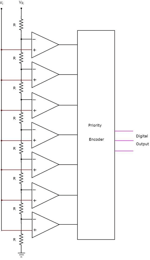
Figure 2: Flash ADC Structure
Main Components of Flash ADC
Resistor Voltage Divider Circuit
A resistor voltage divider circuit is a basic part of Flash ADCs (Analog-to-Digital Converters). It helps lower high input voltages to usable levels in a simple way. This circuit uses a series of resistors to split the voltage, making it easy to control the output voltage by adjusting the resistor values. Using Kirchhoff's Voltage Law, the output voltage can be calculated accurately, which is important for applications that need precise reference voltages.
For example, consider a divider with two resistors, R1 and R2, connected in series. The output voltage (Vout) at their junction is given by the formula Vout = (R2 × Vin) / (R1 + R2). This equation shows the relationship between the input voltage (Vin) and the resistances, demonstrating how the voltage divider changes the voltage output. This mechanism is important for creating stable and accurate voltages for different parts of electronic systems, making the resistor voltage divider a main part of advanced electronic designs.
Comparator
A comparator in a Flash ADC is a main part that helps change analog signals into digital form. It works like a simple amplifier, comparing an input voltage to a reference voltage and giving a binary output that shows the difference between the two. This binary signal is important for digitizing because it tells whether the input voltage is higher or lower than the reference voltage.
The comparator takes the input voltage at its positive input (V+) and the reference voltage at its negative input (V-). The output (Vout) goes high (logic level '1') if V+ is greater than V-, and low (logic level '0') if it's not. This action is required for the ADC because it creates the digital version of the analog signals. By correctly identifying the binary state, the comparator helps the ADC handle different analog signals accurately good for high-quality digital results in electronic devices.
Priority Encoder
The priority encoder makes a Flash ADC work better by making the analog-to-digital conversion process more accurate and reliable. Unlike regular encoders, it handles situations where multiple inputs are high at the same time without confusion. It does this by using a priority system that ranks the inputs, making sure the highest priority signal is always shown in the output.
For example, if a priority encoder with inputs numbered 1 to N detects multiple high inputs like N-1, 4, and 2 at the same time, it will output the binary code for the highest priority input, which is N-1 in this case. This prioritization keeps the ADC's output accurate, which is important for tasks that need precise digital versions of analog signals. The priority encoder considerably improves the overall performance of the device by effectively handling input conflicts, preventing errors and assisting the ADC in operating more effectively and dependably.
Operational Dynamics of Flash ADC
A flash ADC operates by converting an analog input signal into a corresponding digital output in real-time. This process involves a rapid evaluation of the input signal through multiple comparator stages, each tuned to different reference voltage levels. The result is an immediate digital output that directly corresponds to the analog input, showcasing the inherent efficiency and speed of the flash ADC design.
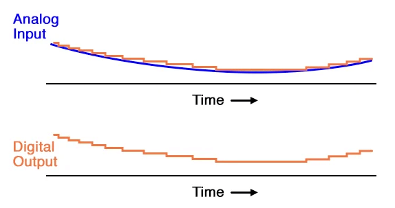
Figure 3: Flash ADC and An Output
Parallel Comparison
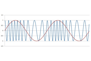
Flash Analog-to-Digital Converters (ADCs) operate using a technique called parallel comparison, which is central to their ability to convert analog signals to digital format rapidly. This method reflects the "flash" in Flash ADC, similar to the quick exposure in photography. At the heart of this mechanism is the simultaneous evaluation of an input analog voltage against multiple reference voltages, derived from a resistor ladder. This component is part for establishing reference benchmarks within the ADC.
Each comparator in the array performs a specific role: comparing the incoming voltage with a designated reference voltage. Conducting these comparisons concurrently enables Flash ADCs to operate at high speeds, a stark contrast to the slower sequential comparisons seen in other ADC types. The outcome of these simultaneous comparisons is a thermometer code, which is a sequence of continuous '1's followed by '0's. For example, in a five-comparator Flash ADC, an input voltage that exceeds the reference voltages of three comparators would result in a thermometer code of 11100. This code format directly converts the analog input into a digital signal, accurately reflecting the amplitude of the input voltage for further digital processing.
Encoding Process
After generating the thermometer code in a Flash ADC, the encoding phase begins. This step is important because it converts the thermometer code into a standard binary format. This reduces the number of output lines needed and makes the digital data easier to manage and process, improving efficiency.
Priority encoding is commonly used for this task. It works by finding the position of the highest '1' in the thermometer code and turning that position into a binary number. For example, in the code 11100, the highest '1' is in the third position, which translates to the binary number 011 in a 3-bit ADC. This method ensures that the most important input is accurately represented and provides a compact digital form of the input voltage. Sometimes, other encoding methods like Gray code are used to reduce errors during signal transfer and processing. Encoding must go rapidly in order to match the high-speed capabilities of Flash ADCs. To achieve this, Flash ADCs use special encoding circuits designed for efficient operation. These circuits allow for fast and accurate encoding, maintaining the device's quick response and high data throughput.
Working of Flash ADCs
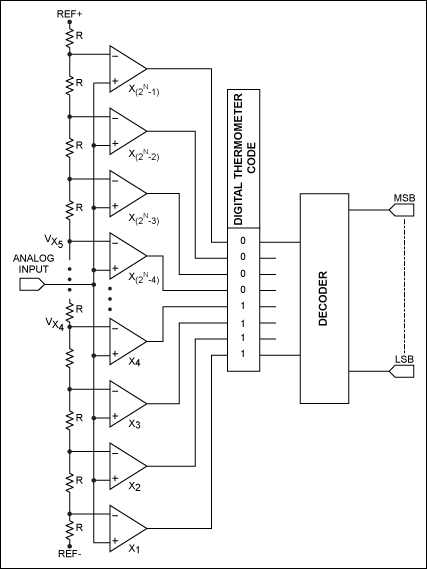
Figure 4: Flash ADC
Flash Analog-to-Digital Converters (ADCs) are best in high-speed digital applications because they quickly convert analog signals into digital formats. In order to quickly convert analog inputs into digital outputs, flash ADCs are constructed with a complex system of high-speed comparators. This network uses a resistive voltage divider to distribute reference voltages across the comparators.
In a flash ADC, each comparator compares the input voltage to a specific reference level. The reference level for each comparator is set by its position in the sequence. For example, in an N-bit flash ADC, there are 2^N - 1 comparators. The reference voltage of each comparator is a little bit (LSB) higher than the previous one. This setup creates a "thermometer code" output pattern, where the binary ones change to zeros at the point where the analog input voltage falls below the comparator's reference voltage. This pattern is similar to how mercury rises in a thermometer, continuously marking higher values until it reaches a point where it stops.
The comparators in a flash ADC are designed to handle high-frequency signals. They typically have wideband, low-gain operational stages to balance bandwidth and gain. Low gain is required at higher frequencies to maintain performance and prevent issues. And, each comparator is designed with a very small voltage offset, smaller than an LSB, to avoid incorrect readings due to minor voltage changes that are not part of the actual signal. To ensure the comparators provide reliable outputs, flash ADCs use regenerative latches at each output stage. These latches employ positive feedback to lock the output state to either 1 or 0. Eliminating any unclear outputs requires this explicit decision-making, particularly in high-speed data conversion.
Optimizing a flash ADC means refining its design by adjusting comparator gain, reducing voltage offset, and improving latch feedback. With these improvements, the flash ADC becomes even more influential in digital electronics by increasing its accuracy, speed, and dependability. With these enhancements, flash ADCs meet higher performance standards, effectively serving advanced digital applications that require quick and accurate analog-to-digital conversion.
A 3-bit Flash ADC Circuit

Figure 5: A 3-bit Flash ADC Circuit
A 3-bit Flash ADC (Analog-to-Digital Converter) circuit is an electronic system used to convert an analog signal into a digital one. Imagine you have a precise and stable reference voltage, known as Vref, which is needed for the ADC's operation. This Vref is supplied by a high-precision voltage regulator that ensures the voltage remains constant and accurate. In this circuit, there are several comparators. Each comparator is a device that compares the input analog voltage with a specific reference voltage level. When the input voltage goes higher than the reference voltage at a particular comparator, that comparator's output switches to a high state, which means it becomes active.
The comparators are arranged in a sequence. So, as the analog input voltage increases, more comparators become active one after another. This sequence of activations indicates the level of the input voltage. The outputs from all these comparators are then sent to a priority encoder. The role of the priority encoder is to examine the active comparator outputs and convert them into a binary number. This binary number represents the highest comparator that is currently active, effectively providing a digital representation of the analog input voltage. So, a 3-bit Flash ADC circuit uses a stable reference voltage to compare against an input voltage. As the input voltage rises, more comparators switch to a high state in sequence. These active states are then encoded into a binary number by the priority encoder, giving a digital output that corresponds to the analog input voltage. This process enables the speedy and effective conversion of analog signals to digital form.
Simplifying Encoder Design in Flash ADC Systems
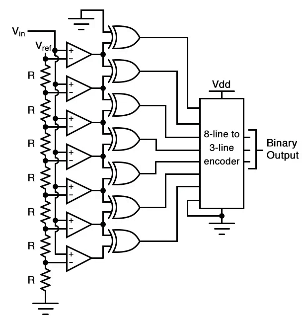
Figure 6: Flash ADC
A priority encoder looks at several inputs and selects the highest-priority one that is active. This selection process helps the system understand which signal to process. However, in some applications, we might not need all the features of a standard priority encoder. In these situations, we can take advantage of a natural characteristic of the comparator outputs in a Flash ADC. Comparators are devices that compare two voltages and output a signal based on which is higher. In a Flash ADC, these comparator outputs often go from low to high in a sequential manner. This means the outputs are naturally ordered from the lowest to the highest.
By using this natural ordering, we can simplify the design. Instead of using a complex priority encoder, we can use a series of Exclusive-OR (XOR) gates. XOR gates are basic logic gates that output true only when the inputs are different. By carefully arranging these XOR gates, we can create an encoding mechanism that effectively selects the highest active input, much like a priority encoder but with less complexity.
This simpler encoding method works well because it leverages the sequential "high" state saturation of the comparator outputs. In essence, the system naturally sorts itself, and the XOR gates just help to read this sorted state. This reduces the overall complexity of the ADC system, making it easier and cheaper to build, while still maintaining its fast performance. Using XOR gates in this way, we can achieve the same effect as a priority encoder, but with fewer parts and less intricate design work.
Constructing Encoder Circuits with Diode Matrices
One efficient and straightforward way to construct an encoder circuit is by using a matrix of diodes. Diodes are electronic components that allow current to flow in one direction while blocking it in the opposite direction. By arranging these diodes in a matrix, you can create a system that interprets different input signals and produces corresponding digital codes. This method is both minimalistic and effective, making it a popular choice for building converter circuits.
The simplicity of using diode matrices means you don't need complex or expensive components. Instead, you can use basic electronic parts to achieve the desired functionality. This practical approach is beneficial for those who are learning about electronics or working on projects with limited resources.
In a flash ADC, speed is important. The encoder circuit must quickly and accurately convert the analog signal into a digital format. Diode matrices are well-suited for this task because they can operate at high speeds, ensuring the overall efficiency of the ADC system. Constructing encoder circuits with diode matrices is a practical and effective method. It allows for the assembly of ADC systems using basic components, making it an accessible option for many electronic enthusiasts and professionals.
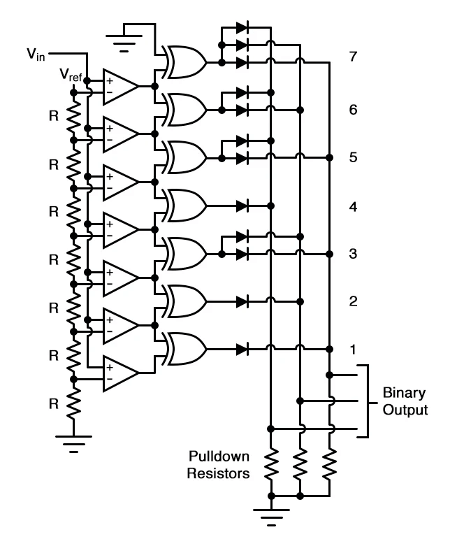
Figure 7: Flash ADC with Diode Matrices
Flash ADC Versus Other ADCs
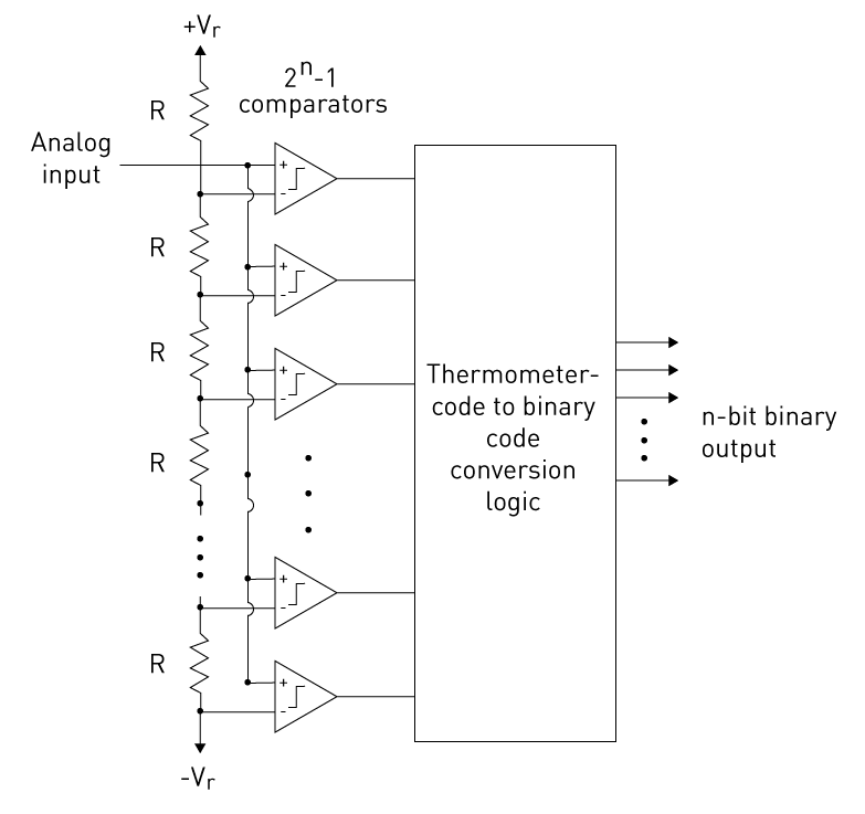
Figure 8: N-bit Flash ADC
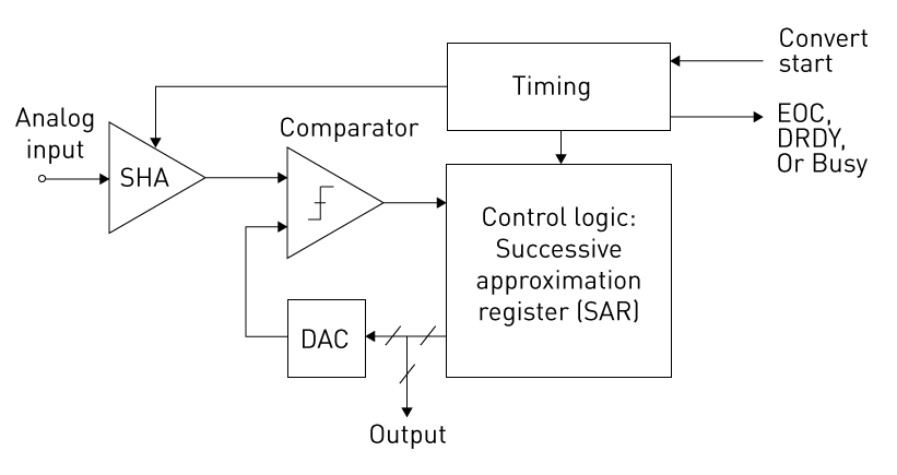
Figure 9: SAR Structure
Flash vs. SAR ADCs
Flash ADCs and SAR ADCs differ greatly in terms of speed, power efficiency, and cost. SAR ADCs work by determining each bit one by one, starting from the most important bit (MSB) to the least important bit (LSB). They use a high-precision comparator that continuously compares against a DAC output, making the process gradual and slower, limiting their speed to a few million samples per second (Msps). On the other hand, Flash ADCs convert the entire analog input to a digital signal in one quick step. This gives them an edge in speed, often achieving speeds in the gigasamples per second (Gsps) range.
For example, SAR ADCs, like the MAX1132, can offer resolutions up to 16 bits. In comparison, Flash ADCs usually provide about 8 bits of resolution. However, this speed comes with a trade-off. An 8-bit SAR ADC, such as the MAX1106, uses only about 100 microamperes (µA) of current at 3.3 volts and operates at a rate of 25 kilosamples per second (ksps). In stark contrast, the Flash ADC MAX104 consumes a hefty 5.25 watts, which is a 16,000-fold increase in power consumption.
Moreover, SAR ADCs are much more cost-effective and come in smaller packages. They are simpler and cheaper to produce, making them a better choice for many applications. Flash ADCs, due to their high power needs, require larger packages to manage heat dissipation and maintain signal integrity. For instance, the MAX104 package is over 50 times larger than that of the MAX1106. This difference in size and power efficiency often makes SAR ADCs the preferred choice in situations like cost and power.
Flash vs. Pipelined ADCs
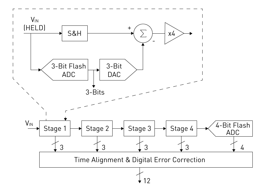
Figure 10: 12-Bit Pipelined ADC
Each has its unique design and characteristics, catering to different needs based on speed, power consumption, and resolution. Pipelined ADCs operate using a parallel processing structure. This means they can handle bits from multiple samples simultaneously across different stages. Each stage processes a portion of the sample before passing it on to the next, allowing for a more continuous flow of data. This design is intended to increase the overall processing speed. However, this parallel processing comes at a cost: pipelined ADCs tend to consume more power and introduce some latency due to the time it takes for each stage to complete its task. For instance, the MAX1449, a type of pipelined ADC, can achieve speeds of up to 100 million samples per second (Msps) with resolutions ranging from 8 to 14 bits. This makes pipelined ADCs suitable for applications requiring moderate to high speeds and resolutions.
On the other hand, Flash ADCs use a simpler approach with straightforward comparators. They can convert an analog signal to a digital one almost instantaneously, making them much faster than pipelined ADCs. Flash ADCs are capable of achieving very high speeds, often several hundred Msps, but they typically offer lower resolutions, up to 10 bits. Their simplicity and speed make them ideal for applications such as in digital oscilloscopes and high-frequency communication systems.
Despite their differences, Flash ADCs and pipelined ADCs can complement each other in hybrid structures. In such configurations, Flash ADCs are integrated into other systems to boost speed while maintaining the desired resolution and accuracy. This synergy allows for enhanced performance, demonstrating how the strengths of each type can be leveraged to meet specific application requirements. While pipelined ADCs are designed for higher resolutions with moderate speeds and involve more complex processing, Flash ADCs excel in achieving very high speeds with simpler design but lower resolution. Understanding their distinct features and applications helps in selecting the right ADC for a given task.
Flash vs. Integrating ADCs
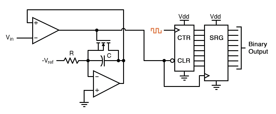
Figure 11: Integrating ADCs
Flash ADCs are incredibly fast at converting analog signals to digital form, making them ideal for tasks that require real-time processing. These tasks include digital oscilloscopes, video signal processing, and radar systems. However, flash ADCs have lower resolution, often ranging from 6 to 8 bits, although higher resolutions are available at a higher cost and with increased complexity. Due to their high speed, flash ADCs consume more power, which can be a drawback in applications where power conservation is important. Also, their complex structure, involving many comparators and resistors, makes them more expensive.
On the other hand, integrating ADCs are slower, operating at a few hundred samples per second or less. This slower speed means they are not suitable for real-time processing. Instead, they are perfect for applications where signals change slowly or require high precision over time, such as monitoring DC signals in industrial settings. Integrating ADCs offer very high resolution, typically 16 bits and above, allowing them to detect small changes in signal levels with great accuracy. They also consume very little power, making them excellent for battery-operated and low-power applications. Furthermore, integrating ADCs are generally more affordable than flash ADCs because their simpler structure involves fewer components.
Flash ADCs are best for high-speed applications that need real-time data conversion, despite their higher power consumption and cost. Integrating ADCs, meanwhile, are ideal for high-resolution, low-speed applications where power efficiency and cost-effectiveness are important.
Flash vs. Sigma-Delta ADCs
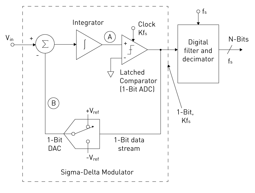
Figure 12: Sigma-Delta ADCs
Sigma-delta ADCs are known for their high resolution. They are designed to work best in situations where precision is more important than speed. These ADCs are typically used for applications with low bandwidth, usually less than 1 MHz. They can achieve very high resolutions, ranging from 12 to 24 bits, by using a process called oversampling. This process involves taking many samples and using noise-reducing filtering techniques to produce a very accurate digital representation of the analog signal. However, sigma-delta ADCs have drawback: they are relatively slow. This makes them less suitable for applications that require high-speed data conversion, especially in multi-channel setups where many signals need to be processed quickly. Despite this limitation, there are ongoing developments in continuous-time sigma-delta ADCs. These advancements aim to improve their speed, potentially making them viable competitors to Flash ADCs in scenarios that need lower data rates but higher resolutions.
Flash ADCs, on the other hand, are built for speed. They can convert analog signals to digital at very high rates, making them ideal for high-frequency environments. However, they typically have lower resolution compared to sigma-delta ADCs. To overcome the speed limitations of sigma-delta ADCs, engineers are exploring ways to integrate Flash ADC modules within sigma-delta systems. This hybrid approach aims to combine the high speed of Flash ADCs with the high resolution of sigma-delta ADCs, resulting in a system that leverages the strengths of both technologies for improved overall performance.
Advantages and Disadvantages of Flash ADCs
|
Aspect |
Details |
|
Speed |
Flash ADCs are known for their fast performance. They compare input voltages against multiple references at the same time, skipping the repeated steps used in other ADCs. This allows Flash ADCs to produce outputs in milliseconds, making them good for immediate data processing needs. |
|
Simplicity |
Flash ADCs are easy to operate. They have only two stages: parallel comparison and encoding. This simplicity makes them easy to understand and operate, reducing design complexity and production costs. However, as resolution increases, more comparators are needed, complicating design and power management. |
|
Scalability and Power Consumption |
Flash ADCs do not scale well. The number of comparators needed increases exponentially with higher resolution, making the design more complex and requiring more power. This high power consumption is problematic for portable devices and environments where managing heat is required. |
|
Complexity for Higher Resolutions |
At higher resolutions, Flash ADCs become very complex. More bits mean more comparators and a more intricate resistor ladder, making power management and layout more challenging. This complexity can reduce efficiency, accuracy, and linearity, and requires precise calibration, increasing both complexity and cost. More components also mean more chip area, which is not ideal for space-limited applications. For high-resolution needs, other ADC technologies like successive approximation or sigma-delta converters are often more cost-effective and scalable. |
Applications of Flash ADC
Communication Systems: Flash ADCs serve a function in high-speed networks such as optical fiber and satellite communications. They convert analog signals to digital form efficiently, enabling quick processing and transmission over long distances. This rapid conversion helps maintain high communication quality, good for applications like real-time broadcasting and high-frequency trading.
Medical Imaging: Flash ADCs are also needed in medical imaging technologies like MRI and CT scanners. These ADCs rapidly convert the analog signals generated by the body into digital data, allowing for the creation of high-resolution images in real time. This quick and accurate data conversion is best for diagnosing and treating medical conditions, especially in urgent situations.
Electronic Warfare: In the field of electronic warfare, Flash ADCs are needed for signal intelligence and electronic countermeasures. These converters quickly turn complex analog signals into digital formats, enabling the military to identify and counteract threats in real time. This capability enhances the strategic and operational responsiveness of military units.
Digital Oscilloscopes: For the purpose of precisely observing the wave form of an electrical signal, digital oscilloscopes require flash ADCs. These ADCs convert high-frequency analog signals into digital form almost instantly. This rapid conversion matters because it ensures that the oscilloscope's digital display is a precise replica of the analog signal. This helps in accurate analysis and measurement of waveforms, making Flash ADCs indispensable for real-time signal processing.
Radar Systems: Radar technology relies heavily on Flash ADCs. Radar systems rely on these converters to quickly change the analog signals, which bounce back from objects, into digital data. Flash ADCs play a major role in electronic warfare signal intelligence and electronic countermeasures. Radar systems require the capacity to detect and monitor objects with high accuracy, need for defense and surveillance operations. Flash ADCs offer this capability by quickly converting signals.
High-Speed Data Acquisition: Flash ADCs are fundamental in fields that require fast data collection, such as scientific research, industrial monitoring, and automated testing. These converters are designed to capture quickly changing signals without losing important information. This high-speed data acquisition is required for accurate analysis and monitoring in applications where signal integrity is important.
Conclusion
Flash ADCs represent the peak of speed in analog-to-digital conversion technology with their simple yet powerful design that allows for fast signal processing. This article has shown their different role in high-speed, real-time applications, where quick conversion from analog to digital is needed. While Flash ADCs are straightforward in their operation, they face challenges in scaling up resolution, requiring more complex designs and higher power use. This balance between speed and the trade-offs in power efficiency and design complexity is important in ADC technology. As the need for faster and more efficient electronics grows, Flash ADCs will play a major role in the future of digital electronics, balancing speed, resolution, and power efficiency to meet the needs of both industrial and consumer technology.
Frequently Asked Questions [FAQ]
1. Why is a Flash ADC Faster?
A flash ADC, also known as a parallel ADC, is faster than other types of ADCs because it processes all bits of the input signal simultaneously. This parallel processing is achieved by using a series of comparators that each check whether the input voltage is above or below certain reference levels. Since it performs all comparisons at once and directly outputs the digital value, a flash ADC eliminates the need for sequential approximation or iterative conversion processes found in other ADC types. This design allows for nearly instantaneous conversion, making flash ADCs the fastest type available.
2. What is a 2-bit Flash ADC?
A 2-bit flash ADC is a type of analog-to-digital converter that quantizes an analog input signal into one of four possible digital outputs (00, 01, 10, or 11). It utilizes three comparators, each comparing the input signal to a different reference voltage. The outputs of these comparators are then decoded into a 2-bit digital value. This ADC is capable of representing the analog input with a resolution of four levels.
3. What is a 3-bit Flash ADC?
A 3-bit flash ADC expands upon the 2-bit version by providing an even finer resolution. It converts an analog input into one of eight possible digital outputs (ranging from 000 to 111). This type of ADC uses seven comparators, each set to a distinct reference voltage. The comparators simultaneously assess whether the input voltage is higher or lower than their respective references, and the results are then converted into a 3-bit digital code, enabling the representation of the analog input at eight different levels.
4. Where is Flash ADC Used?
Applications that require quick data conversion and high speed are the main ones that employ flash ADCs. Common use cases include digital video broadcasting, radar systems, and high-frequency signal processing. They are perfect for settings where response time matters greatly because of their near-instantaneous conversion of analog signals to digital form.
5. How is an Analog Signal Converted into Digital with Flash Type ADC?
In a flash ADC, the analog input signal is fed to a series of comparators. Each comparator has a reference voltage that divides the input voltage range into equal segments. All comparators operate simultaneously, each delivering a binary output of '1' if the input exceeds its reference voltage and '0' otherwise. These binary outputs are then combined in a logic circuit, which translates the comparator outputs into a binary number that represents the digital equivalent of the analog input.
6. How Many Bits is a Flash ADC?
The number of bits in a flash ADC defines its resolution, i.e., how finely it can divide the analog input range and represent it as a digital output. Flash ADCs can vary widely in their resolution, commonly ranging from 2 bits to as many as 10 bits or more, depending on the specific application and the required precision.
7. What is the Speed of Flash ADC?
The speed of a flash ADC is primarily determined by how quickly its comparators can settle and its logic circuitry can encode the output. Typically, flash ADCs can achieve conversion times on the order of nanoseconds. For instance, a high-speed flash ADC might offer speeds ranging from 500 megasamples per second (Msps) to over several gigasamples per second (Gsps), making them exceptionally fast compared to other ADC types. Applications that need real-time processing and low latency depend on this performance.
About us
ALLELCO LIMITED
Read more
Quick inquiry
Please send an inquiry, we will respond immediately.
Exploring the Rectification Properties of PN Junctions
on June 24th
How to Read an Ohmmeter Resistance Measurement?
on June 22th
Popular Posts
-
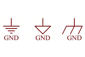
What is GND in the circuit?
on January 1th 2946
-

RJ-45 Connector Guide: RJ-45 Connector Color Codes, Wiring Schemes, R-J45 Applications, RJ-45 Datasheets
on January 1th 2502
-

Fiber Connector Types: SC Vs LC And LC Vs MTP
on January 1th 2091
-
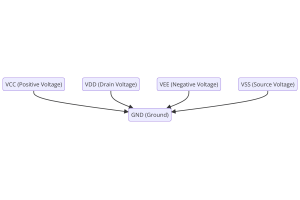
Understanding Power Supply Voltages in Electronics VCC, VDD, VEE, VSS, and GND
on November 9th 1898
-

Comparison Between DB9 and RS232
on January 1th 1765
-

What Is An LR44 Battery?
Electricity, that ubiquitous force, quietly permeates every aspect of our daily lives, from trivial gadgets to life-threatening medical equipment, it plays a silent role. However, truly grasping this energy, especially how to store and efficiently output it, is no easy task. It is against this background that this article will focus on a type of coin cell battery that may seem insignificant on the...on January 1th 1714
-
Understanding the Fundamentals:Inductance Resistance, andCapacitance
In the intricate dance of electrical engineering, a trio of fundamental elements takes center stage: inductance, resistance, and capacitance. Each bears unique traits that dictate the dynamic rhythms of electronic circuits. Here, we embark on a journey to decipher the complexities of these components, to uncover their distinct roles and practical uses within the vast electrical orchestra. Inductan...on January 1th 1662
-

CR2430 Battery Comprehensive Guide: Specifications, Applications and Comparison to CR2032 Batteries
What is CR2430 battery ?Benefits of CR2430 BatteriesNormCR2430 Battery ApplicationsCR2430 EquivalentCR2430 VS CR2032Battery CR2430 SizeWhat to look for when buying the CR2430 and equivalentsData Sheet PDFFrequently Asked Questions Batteries are the heart of small electronic devices. Among the many types available, coin cells play a crucial role, commonly found in calculators, remote controls, and ...on January 1th 1567
-
What Is RF and Why Do We Use It?
Radio Frequency (RF) technology is a key part of modern wireless communication, enabling data transmission over long distances without physical connections. This article delves into the basics of RF, explaining how electromagnetic radiation (EMR) makes RF communication possible. We will explore the principles of EMR, the creation and control of RF signals, and their wide-ranging uses. The article ...on January 1th 1550
-

CR2450 vs CR2032: Can The Battery Be Used Instead?
Lithium manganese batteries do have some similarities with other lithium batteries. High energy density and long service life are the characteristics they have in common. This kind of battery has won the trust and favor of many consumers because of its unique safety. Expensive tech gadgets? Small appliances in our homes? Look around and you'll see them everywhere. Among these many lithium-manganes...on January 1th 1519
HOT Part Number
-

MC74HC4051ADR2G
Fairchild Semiconductor
SINGLE-ENDED MULTIPLEXER, 8 CHAN
GRM155R61H333KE19D
Murata Electronics
CAP CER 0.033UF 50V X5R 0402
1N5712
Microchip Technology
DIODE SCHOTTKY 20V 75MA DO35
PC3H711NIP
Sharp Microelectronics
OPTOISO 2.5KV TRANS 4-MINI-FLAT
A1106EUA-T
Allegro MicroSystems
MAGNETIC SWITCH UNIPOLAR 3SIP
BD9106FVM-TR
Rohm Semiconductor
IC REG BUCK ADJ 800MA 8MSOP
GRM1885C2A1R0BA01D
Murata Electronics
CAP CER 1PF 100V C0G/NP0 0603
AD8531AKS-REEL7
Analog Devices Inc.
IC OPAMP GP R-R CMOS 3MHZ SC70-5
BTA08-600BWRG
STMicroelectronics
TRIAC ALTERNISTOR 600V TO220AB
TL084QDR
Texas Instruments
IC OPAMP JFET 4 CIRCUIT 14SOIC
GRM0335C1H6R1CD01D
Murata Electronics
CAP CER 6.1PF 50V C0G/NP0 0201
NF4EB-5V
Panasonic Electric Works
RELAY GEN PURPOSE 4PDT 2A 5VDC
NDF10N60ZG
onsemi
MOSFET N-CH 600V 10A TO220FP
C1005C0G1H360J
TDK Corporation
CAP CER 36PF 50V C0G 0402
XC6216D502MR-G
Torex Semiconductor Ltd
IC REG LINEAR 5V 150MA SOT23
UCC3913DTR
Texas Instruments
IC HOT SWAP CTRLR -48V 8SOIC
170M3810D
Eaton - Bussmann Electrical Division
FUSE SQUARE 63A 700VAC RECT
C0603C0G1E7R5C
TDK Corporation
CAP CER 7.5PF 25V C0G 0201 -
2007198-2
TE Connectivity AMP Connectors
CONN SFP+ CAGE PRESS-FIT R/A
UCC561DP
Unitrode
TERMINATOR SUPPORT CIRCUIT, 27-L
CC2640R2FYFVR
Texas Instruments
IC RF TXRX+MCU BLE 5.1 34DSBGA
MSP430F2001IN
Texas Instruments
IC MCU 16BIT 1KB FLASH 14DIP
NVMFD5485NLT3G
onsemi
MOSFET 2N-CH 60V 5.3A DFN8
LTC1420IGN#TRPBF
Analog Devices Inc.
IC ADC 12BIT PIPELINED 28SSOP
1206AC470KAT9A
KYOCERA AVX
CAP CER 47PF 1KV X7R 1206
GRT21BR60G476ME13L
Murata Electronics
CAP CER 47UF 4V X5R 0805
VE-JW3-IX
Vicor Corporation
DC DC CONVERTER 24V 75W
TPS73633DBVR
Texas Instruments
IC REG LINEAR 3.3V 400MA SOT23-5
CA3085E
Harris Corporation
IC REG LINEAR POSITIVE VOLTAGE
SN74ALS641AN
Texas Instruments
IC TRANSCEIVER INVERT 5.5V 20DIP
BCM6303KMLG
Broadcom Limited
XDSL CPE LINE DRIVER W/ ON-CHI
RT9017-20GBR
Richtek USA Inc.
IC REG LINEAR 2V 500MA SOT23-5R
VI-2WZ-CW
Vicor Corporation
DC DC CONVERTER 2V 20W
IXTL2X200N085T
IXYS
MOSFET 2N-CH 85V 112A I5-PAK
P6SMB36AT3G
Littelfuse Inc.
TVS DIODE 30.8VWM 49.9VC SMB
TPA2011D1YFFR
Texas Instruments
IC AMP CLASS D MONO 3.24W 9DSBGA -
2N5886
Microchip Technology
PNP POWER TRANSISTOR SILICON AMP
200096-0101
Molex
Automotive Connectors TAK50 RCPT
SP708RCN-L
Sipex
POWER SUPPLY SUPPORT CIRCUIT, FI
LT1885CS#TRPBF
Analog Devices Inc.
IC OPAMP GP 4 CIRCUIT 14SO
EFM32G290F128-BGA112
Silicon Labs
IC MCU 32BIT 128KB FLASH 112BGA
GRM1556S1H1R2CD01D
Murata Electronics
CAP CER 1.2PF 50V S2H 0402
CC0603JRX7R9BB391
YAGEO
CAP CER 390PF 50V X7R 0603
ATF16V8B-15JI
Microchip Technology
IC PLD 8MC 15NS 20PLCC
BTS240AHKSA1
Infineon Technologies
N-CHANNEL POWER MOSFET
TSH62CDT
STMicroelectronics
IC OPAMP GP 2 CIRCUIT 8SOIC
AD7534KN
Analog Devices Inc.
IC DAC 14BIT A-OUT 20DIP
SGL40N150DTU
Fairchild Semiconductor
N-CHANNEL IGBT
SBL1060CTP
Diodes Incorporated
DIODE ARRAY SCHOTTKY 60V ITO220S
12061C822JAT2A
KYOCERA AVX
CAP CER 8200PF 100V X7R 1206
NE5532APSR
Texas Instruments
IC OPAMP GP 2 CIRCUIT 8SO
TLV2460IDBVT
Texas Instruments
IC OPAMP GP 1 CIRCUIT SOT23-6
BZX84-B5V1215
NXP USA Inc.
DIODE ZENER 5.1V 250MW TO236AB
L78L12ACZ
STMicroelectronics
IC REG LINEAR 12V 100MA TO92-3