Exploring the Rectification Properties of PN Junctions
The development of semiconductor technology has played a key role in the evolution of modern electronics, largely influenced by the advancement and insights into the P-N junction. This article explores the operational principles and applications of P-N junctions, juxtaposing them with the technological ingenuity of the crystal radio. Initially, it explores the crystal radio, a clever device that operates without external power, utilizing the semiconductive nature of galena (lead sulfide). This precedes a more detailed examination of the P-N junction, a dominant element in today's electronic devices, primarily functioning as a rectifier diode.The analysis of forward and reverse bias operations within the article demonstrates how these processes allow the junction to manage electrical current flow in electronic circuits. In addition, it explores the P-N junction's behavior under various conditions and voltages, including its use in devices like Zener diodes and rectifiers. This thorough review not only highlights the physical and electronic mechanisms of P-N junctions but also emphasizes their dynamic role in rectification and voltage regulation.
Catalog
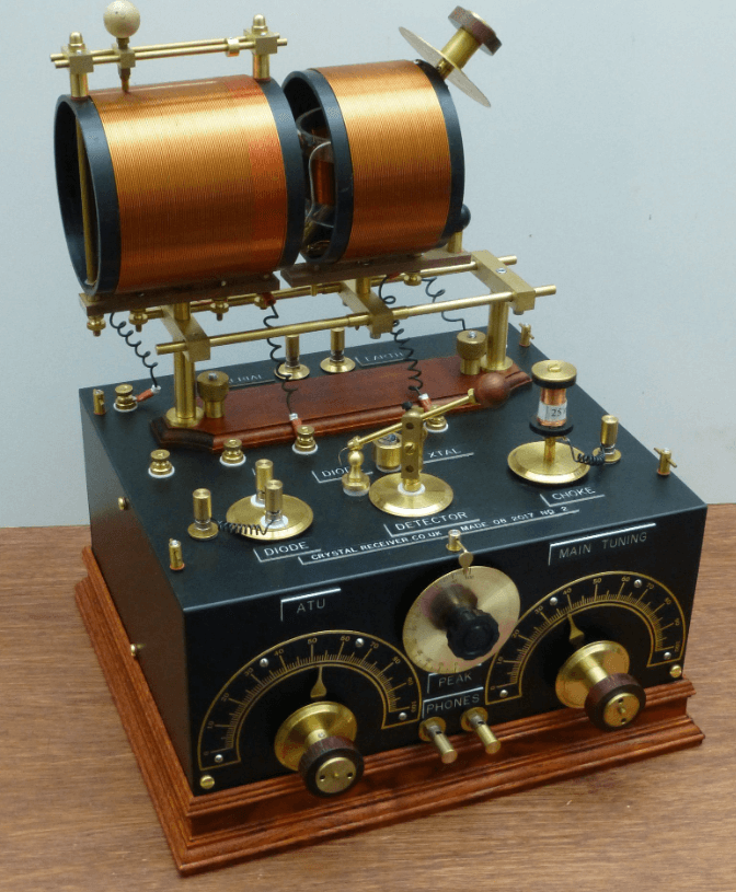
Figure 1: Cyrstal Radio
Exploring the Crystal Radio
The Crystal Radio, an early marvel of radio technology, used natural semiconductors like galena (lead sulfide) to work without any external power source. Galena, with its crystalline structure, is an early example of modern semiconductors due to its natural ability to rectify, which is needed for diodes today.
Galena's semiconductive properties, including an energy gap of about 0.4 electron volts (eV), are dynamic for its function. This gap between the valence and conduction bands, combined with small impurities, helps excite electrons, allowing them to move into the conduction band and conduct electricity. This mechanism enabled the crystal radio detector to convert alternating current (AC) from the antenna into usable direct current (DC). More prominently, it demodulated amplitude-modulated (AM) signals, extracting audio signals from radio waves.
In a crystal radio, the antenna captures radio frequency signals and directs them to a tuning coil to select the desired frequency. The selected signal then meets the galena detector. Here, rectification occurs, converting AC into a modulated DC signal. This signal is then sent to a headset or speaker, where the audio modulation becomes audible, completing the signal translation without external power.
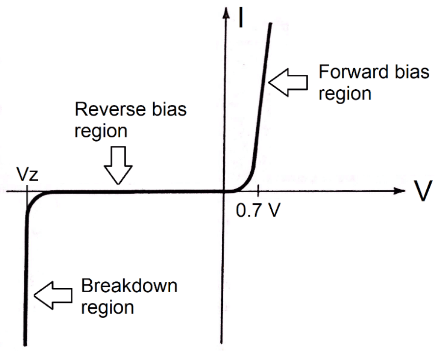
Figure 2: P-N Rectifying Junction
Understanding the P-N Rectifying Junction
The P-N junction is ultimate to modern electronics, primarily functioning as a rectifier diode. It allows current to flow in one direction, which is needed for converting alternating current (AC) to direct current (DC).
Structure and Function
The P-N junction consists of p-type and n-type semiconductor materials. The p-type has an excess of holes, while the n-type has an excess of electrons. Where these materials meet, a depletion zone forms, creating a built-in potential barrier that prevents the free flow of charge carriers between the regions.
When a positive voltage is applied to the p-side relative to the n-side (forward bias), the potential barrier lowers, allowing current to flow easily across the junction. When a negative voltage is applied (reverse bias), the barrier heightens, blocking current flow. This selective conductivity is what enables the diode to convert AC into DC.
The P-N junction diode is strategically placed in the circuit to align with the intended direction of the current flow. An AC voltage is then applied to the circuit. During each AC cycle, the diode functions by either blocking or allowing current to pass through. This selective passage, dependent on the diode's orientation, permits only half of the AC cycle to pass, resulting in a pulsating DC output. To transform this pulsating DC into a more stable and consistent DC voltage, components like capacitors and voltage regulators are employed to smooth out the output.
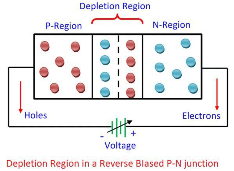
Figure 3: P-N Junction with Reverse Bias
Analyzing the P-N Junction Under Reverse Bias
Reverse biasing a P-N junction involves connecting the negative terminal of a DC battery to the P-type semiconductor and the positive terminal to the N-type semiconductor. This configuration enhances the electric field across the junction, pushing the majority of carriers—holes in the P-type and electrons in the N-type—away from the junction. This migration increases the width of the depletion zone, an area void of free charge carriers, effectively widening the barrier that impedes charge carrier movement.
In this state, the flow of current across the junction is minimal and mainly results from thermally generated electron-hole pairs within the semiconductor material. When in reverse bias, minority carriers, such as holes in the N-type and electrons in the P-type, are drawn towards the junction, creating a consistent, albeit small, reverse saturation current (IS). This current slightly increases with temperature as more charge carriers are generated, yet it remains relatively stable regardless of further increases in reverse bias voltage, which explains its characterization as a "saturation" current.
By applying reverse bias, the potential barrier at the junction is enlarged, significantly enhancing the barrier voltage to V0 + V, where V0 is the contact potential and V is the applied voltage. This higher barrier drastically reduces the diffusion current of the majority carriers, nearly eliminating it at a reverse bias of about one volt, leaving only the reverse saturation current active. This results in a high junction resistance, proving dynamic for applications such as voltage regulation and signal modulation, where the junction’s high impedance restricts current flow. The sensitivity of the reverse saturation current to temperature variations also enables the junction to function as a basic sensor, monitoring changes for temperature-sensitive applications.
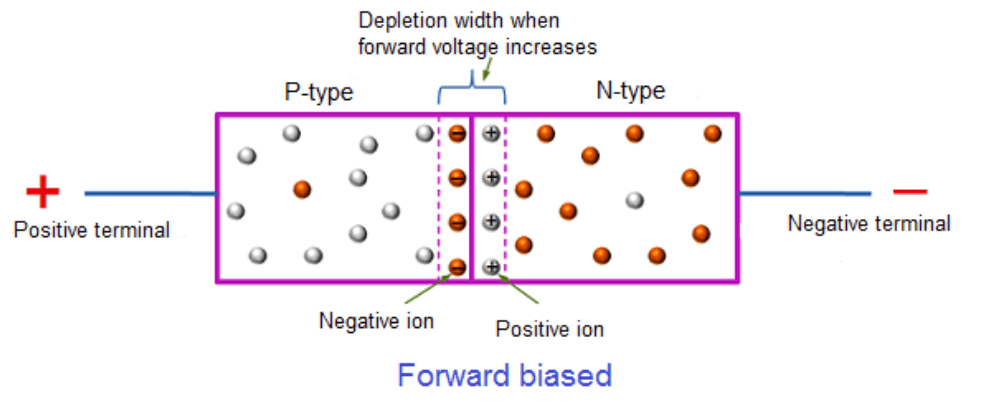
Figure 4: P-N Junction with Forward Bias
Examining the P-N Junction Under Forward Bias
In a forward-biased P-N junction, the DC battery's positive terminal connects to the P-type semiconductor, and the negative terminal connects to the N-type semiconductor. This setup makes the P-type side more positive compared to the N-type side. Under these conditions, the majority of carriers (holes in the P-type and electrons in the N-type) are driven towards the junction.
The electric field created by the battery pushes the majority of carriers away from their respective terminals and towards the junction. As these carriers move and converge at the junction, they recombine. This recombination significantly reduces the width of the depletion region, facilitating a stronger flow of carriers across the junction.
The applied forward voltage V lowers the junction's potential energy barrier. Normally, this barrier prevents free carrier flow, but the forward voltage reduces the barrier to V0 - V1 where V0 is the built-in potential of the junction. This lowered barrier height allows more electrons and holes to diffuse across the junction.
Lowering the barrier height results in a substantial increase in the diffusion current (Id) which is the flow of charge carriers driven by the reduced barrier. This flow is primarily in one direction, with the majority of carriers moving towards and through the junction. The current in this forward-biased state is significantly higher than the reverse saturation current (Is) observed under reverse bias.
This sequence of operations ensures that the P-N junction effectively converts the battery's voltage into a high flow of electrical current through the semiconductor. This is useful for devices like diodes and transistors, where controlled current flow is a must. The forward-biased P-N junction's ability to support a high diffusion current makes it an unsafe component in various electronic applications, from rectification to signal amplification.
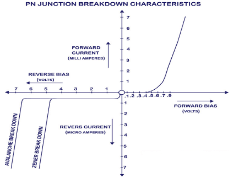
Figure 5: Junction Breakdown
Breakdown Phenomena in P-N Junctions
Junction breakdown in a P-N junction occurs when the reverse voltage applied across the junction exceeds a specific threshold, known as the breakdown voltage (VBR) or Zener voltage (Vz). This phenomenon results in a dramatic increase in reverse current without a significant rise in voltage. Devices like Zener diodes exploit this characteristic for voltage regulation, managing the event without damage.
In a reverse-biased P-N junction, a small current called reverse saturation current (Is) flows due to thermally generated carriers. As the reverse voltage increases, the potential barrier at the junction rises, suppressing the diffusion current (Id) until it effectively becomes zero. This leaves only (Is) to sustain the current flow.
Increasing Reverse Voltage and Depletion Region Widening
As the reverse voltage continues to increase, the depletion region widens. When the voltage at the junction reaches VBR or Vz , the electric field within the depletion region becomes intense enough to initiate junction breakdown. This breakdown occurs through either the Zener effect or the avalanche effect, resulting in a significant increase in current.
Zener Effect: The Zener effect is dominant at lower breakdown voltages, typically below 5V in silicon. It involves the quantum mechanical tunneling of electrons across the depletion region. The intense electric field in the depletion layer is strong enough to strip electrons from their atomic bonds, creating electron-hole pairs. These carriers are then swept across the junction by the field, substantially increasing the reverse current.
Avalanche Effect: At higher voltages, generally above 7V, the avalanche effect predominates. Minority carriers (electrons in the P-type region and holes in the N-type region) gain kinetic energy from the electric field as they cross the depletion region. If these carriers acquire sufficient energy, they can collide with lattice atoms, releasing additional electron-hole pairs. This secondary generation of carriers can lead to further collisions, creating a chain reaction—an avalanche—thus magnifying the reverse current.
The junction's ability to sustain breakdown without damage depends on effective thermal management and the robustness of its physical and electronic structure. The specific breakdown mechanism—whether Zener or avalanche—depends on the material properties of the semiconductor, such as band gap and doping levels, and external conditions like temperature.
The Process of Rectification Explained
The rectification process in a P-N junction relies on its non-linear, or non-ohmic, behavior. This is evident in the volt-ampere characteristic curve, which shows the junction's asymmetric response to voltage: reversing the voltage polarity does not produce the same current in the opposite direction. This asymmetry is needed for rectifying devices.
Understanding the Behavior
When a sinusoidal input voltage with an amplitude V0 is applied to a P-N junction, the junction's response is shown on the characteristic curve. The output current oscillates between I1 (during forward bias) and -I2 (during reverse bias). The key point is that I1 (forward current) is much larger than -I2 (reverse current). This difference in current magnitudes between forward and reverse biases enables rectification.
Forward and Reverse Bias Effects
Under forward bias, the P-N junction allows a large current (Id) to flow because the forward voltage reduces the potential barrier. This reduction permits majority carriers (electrons and holes) to move freely across the junction, generating substantial current. In reverse bias, the potential barrier increases, severely restricting the flow of carriers and thus the current. The current during reverse bias (Is) is minimal compared to the forward bias current.
Conversion of AC to DC
This behavior—allowing significant current in one direction while restricting it in the other—effectively converts alternating current (AC) input into direct current (DC) output. The rectification process depends on the P-N junction's asymmetric conductivity in response to alternating voltage. This makes it a significant component in power supplies and signal modulation applications, where unidirectional current flow is a must.
Role of P-N Rectifying Junction Technology in Rectifiers
A P-N junction, needed for diodes, allows current to flow mainly in one direction due to its unique conduction properties under different electrical biases.
In reverse bias, connect the battery's negative terminal to the P-type side and the positive terminal to the N-type side. This setup increases the junction’s built-in potential, widening the depletion zone and greatly reducing the diffusion current. The drift current, however, remains unaffected, resulting in a small, nearly constant reverse saturation current (Id). The expanded depletion zone under reverse bias acts as a barrier, restricting the flow of charge carriers and allowing minimal current to pass.
In forward bias, connect the battery's positive terminal to the P-type side and the negative terminal to the N-type side. This setup lowers the potential barrier at the junction, narrowing the depletion zone. The reduced barrier height allows more majority carriers (electrons in the N-type and holes in the P-type) to cross the junction, significantly increasing the diffusion current (Id). In this configuration, the drift current of minority carriers remains largely unaffected. The narrowing of the depletion zone under forward bias enhances the junction's conductivity, allowing a substantial flow of diffusion current, which is the primary current in this mode.
When subjected to high reverse biases, typically several hundred volts, the P-N junction can endure extreme conditions. Under such voltages, the intense electric field across the depletion zone can generate significant numbers of electron-hole pairs, potentially leading to a sharp increase in current and causing junction breakdown. This state is generally avoided in standard semiconductor diodes due to the risk of permanent damage. However, Zener diodes are designed to operate reliably in this breakdown region for applications like voltage regulation.
The resistance of the P-N junction varies with the magnitude and polarity of the applied voltage. This variation allows preferential current flow in the forward direction while blocking it in reverse. This directional current flow underpins the junction's role as a rectifier in various electronic circuits, from power supplies to signal processing systems.
Applications of P-N Junction Diodes as Rectifiers
The P-N junction diode's inherent ability to allow current to flow in one direction makes it an effective rectifier, converting alternating current (AC) into direct current (DC). The simplest form of such a device is the half-wave rectifier.
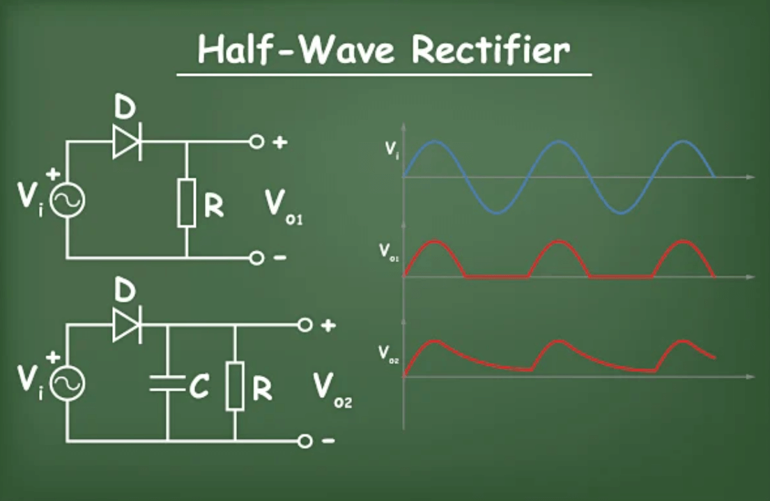
Figure 6: Half-Wave Rectification Process
In a half-wave rectifier circuit, the diode functions during the AC input signal's positive and negative half-cycles. This setup typically includes a transformer with a secondary coil that induces an electromotive force (EMF) through mutual induction with the primary coil. The polarity of the induced EMF changes with the AC cycle.
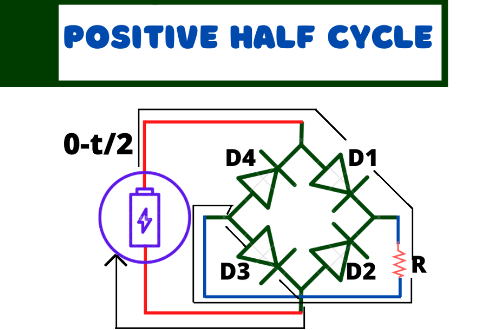
Figure 7: Positive Half-Cycle
The upper end of the secondary coil becomes positively charged relative to the lower end, which forward biases the P-N junction diode. This biasing allows current to flow through the load resistance (RL). As the current flows, a voltage is observed across RL, corresponding to the positive half-cycle of the AC input.
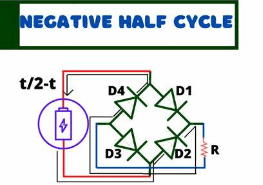
Figure 8: Negative Half-Cycle
When the polarity of the induced EMF reverses, the upper end becomes negative and the lower end positive. These reverse biases the diode, effectively blocking the current flow through it. As a result, no output is obtained across the load resistance during this half-cycle.
Characteristics and Output of the Half-Wave Rectifier
The half-wave rectifier converts only the positive half-cycles of the AC input into a pulsating DC output. This output contains AC components and is inherently discontinuous with lower efficiency compared to full-wave rectifiers. The pulsating nature of the output can be quantified by calculating the mean load current. Multiplying this current by the load resistance (RLR_LRL) gives the average output DC voltage.
The main drawbacks of the half-wave rectifier are its inefficiency and the discontinuous nature of the output. Further filtering or smoothing may be required to achieve a steady DC supply. The rectifier's performance and efficiency are influenced by the diode's characteristics, such as its forward voltage drop and reverse leakage current. In addition, the design of the transformer and the choice of load resistance are significant in optimizing the rectifier's overall functionality.
Conclusion
This article's examination of the P-N junction highlights both its wide range of uses in contemporary electronics and its key role in the development of semiconductor technology. From the basic operation of a crystal radio to the sophisticated mechanisms of junction breakdown and rectification, the P-N junction emerges as the ultimate component in ensuring directional current flow and stable voltage outputs in electronic circuits. The detailed examination of both forward and reverse bias operations illustrates the junction’s versatility in adapting to different electrical stresses and environmental conditions. The practical applications of the P-N junction, as demonstrated in rectifiers and voltage regulators, emphasize its serious function in enhancing the efficiency and reliability of electronic devices. Ultimately, this in-depth analysis not only clarifies the operational principles of P-N junctions but also showcases their key role in advancing technology from simple radios to complex integrated circuits, marking a significant epoch in the field of electronics.
Frequently Asked Questions [FAQ]
1. How is a PN junction used as a rectifier?
A PN junction forms when p-type and n-type semiconductor materials are joined. This junction naturally creates a depletion region that acts like a barrier, allowing current to flow more easily in one direction than the other. When AC voltage is applied to a PN junction, during the positive half-cycle, the junction allows the current to pass (forward-biased), and during the negative half-cycle, it blocks the current (reverse-biased). This selective conduction results in the output being predominantly in one direction, effectively converting AC to DC.
2. What is the common purpose of a rectifier PN junction?
The primary purpose of a rectifier PN junction is to produce a steady DC output from an AC input. This is needed in powering electronic circuits that require DC for stable operation. Rectifiers are ultimate in power supply units for all kinds of electronic and electrical devices, from small gadgets to large industrial machines.
3. What is the rectifying application of the PN junction diode?
The PN junction diode is specifically designed to exploit the rectifying behavior of the PN junction. It is widely used in circuits as a rectifier to perform this key function of AC to DC conversion. In practical terms, these diodes are found in chargers for batteries, power adapters, and systems that require a reliable DC supply from an AC source, such as telecommunications equipment and automotive electrical systems.
4. What is the PN junction used for?
Besides rectification, PN junctions are used in various other applications such as signal modulation, voltage regulation, and light-emitting diodes (LEDs) for illumination and displays. However, their most significant and widespread use remains in rectification, where they are useful components in converting AC into usable DC power.
5. How does a diode act as a rectifier?
A diode, which consists of a PN junction, acts as a rectifier by allowing electric current to flow more easily in one direction than in the reverse direction. The inherent properties of the PN junction, primarily the one-way flow feature, make diodes ideal for blocking the negative part of AC signals, thereby allowing only the positive part to pass. This selective passage of current results in the output being a unidirectional flow of electrons or DC.