Understanding the Buck Converters: Work Principle, Designing, and Operation
Buck converters, commonly referred to as step-down voltage regulators, have become dynamic components in the field of modern electronics as they enable effective power control. Through detailed analysis, we will explore the two-phase operation of buck converters, their waveforms, and the transfer function that dictates their behavior. In addition, we will examine the different types of buck converters, their conduction modes, and the specific applications that benefit from their use. We may recognize the key role that buck converters play in contemporary electronic systems and their contribution to dependability and energy efficiency by comprehending these basic concepts.Catalog
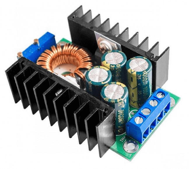
Figure 1: Buck Converter
Basics of Buck Converters
Buck converters, also called step-down voltage regulators, are fundamental in modern electronics, efficiently converting voltage for various uses. These DC-DC converters primarily use transistor switches like MOSFETs, IGBTs, or BJTs paired with an inductor to precisely manage power and lower voltage levels.
Here’s a detailed breakdown of how buck converters operate:
Energy Storage - When the transistor switch is closed, current flows through the inductor, storing energy in its magnetic field.
Energy Transfer - When the switch opens, the inductor releases its stored energy to the output and load. A diode prevents the current from flowing back, ensuring stable output.
Output Filtering - An output capacitor smooths the pulsed output from the inductor, converting it into a steady DC voltage safe for sensitive electronic components.
How a Buck Converter Works?
Understanding a buck converter involves a detailed look at its precise two-phase operation. This process relies on the coordinated actions of the output capacitor, inductor, and switch. The system not only reduces voltage but also stabilizes the output against inherent fluctuations.
When the switch (typically a transistor like a MOSFET) is turned on, it allows current to flow from the power source into the inductor and the output capacitor. The inductor regulates the current flow rate, preventing the capacitor from charging too quickly.
When the switch is turned off, the inductor, which opposes sudden changes in current, generates a reverse electromotive force (back EMF). This uses its stored magnetic energy to keep current flowing to the load. During this phase, a diode becomes requisite, allowing current to bypass the open switch and maintain a continuous flow to the load and capacitor. This action is decisive for sustaining steady output voltage and current.
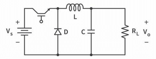
Figure 2: Circuit Diagram of Buck Converters
Circuit Diagrams of Buck Converters
A buck converter circuit consists of key components: a MOSFET switch, an inductor, a diode (or an additional MOSFET in some advanced designs), and a capacitor. When these parts are combined into a straightforward circuit architecture and integrated with a control circuit, they form a fully functional buck regulator.
MOSFET Switch: The MOSFET switch is the primary control element. The control circuit adjusts the MOSFET's duty cycle by continuously monitoring the output voltage against a reference value. This adjustment ensures that the output voltage stays constant despite variations in load or input voltage.
Inductor: Placed between the input voltage source and the load, the inductor stores and delivers energy. During the MOSFET's 'on' phase, it stores energy in its magnetic field. When the MOSFET turns 'off', the stored energy is released to the load, providing a continuous supply even when there is no direct input power.
Diode: The diode maintains unidirectional current flow, especially during the MOSFET's 'off' phase, preventing reverse current that could destabilize the circuit. In some designs, a second MOSFET replaces the diode to enhance efficiency by reducing losses during high-frequency switching.
Output Capacitor: The capacitor smooths out voltage ripple, stabilizing the output voltage by filtering fluctuations caused by the switching process. This ensures the load receives a consistent and stable voltage.
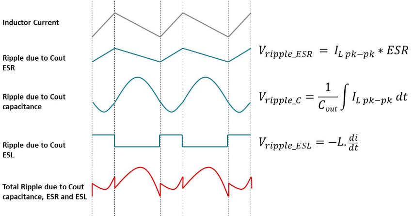
Figure 3: Buck Converter Electrical Waveforms
Electrical Waveforms in Buck Converters
The waveform of a buck converter shows the details of its operation, illustrating key electrical properties like input voltage (Vin), output voltage (Vout), switch node voltage (Vsw), inductor current (IL), and diode current (ID). These parameters help us understand the electrical interactions within the converter during each switching cycle.
Input Voltage (Vin): This voltage remains relatively steady during operation and acts as the main power source for the converter.
Output Voltage (Vout): The output voltage is regulated to be lower than the input voltage and is controlled by the switch's duty cycle. Its stability matters to the downstream devices' safe operation. The ripple in Vout is influenced by the characteristics of the output capacitor and the inductor.
Switch Node Voltage (Vsw): The voltage at the switch node changes significantly based on the switch state (MOSFET). When the switch is 'on', Vsw is nearly equal to Vin. When the switch is 'off', Vsw drops to a value slightly above ground, determined by the diode's forward voltage drop or zero, depending on the circuit.
Inductor Current (IL): The current through the inductor increases linearly when the switch is 'on' because energy is being stored in the inductor's magnetic field. When the switch is 'off', IL decreases as energy is transferred to the output load and capacitor. The smooth transition of IL between these states minimizes output voltage ripple and enhances efficiency.
Diode Current (ID): The current through the diode flows only when the switch is 'off'. This allows the inductor to discharge its stored energy to the output. In designs with a synchronous rectifier (using a second MOSFET instead of a diode), this phase is managed by the second MOSFET, which reduces losses and can increase efficiency.
Switching Frequency (fsw): The switching frequency, ranging from tens of kilohertz to several megahertz, affects the converter's performance, including efficiency, the size of the reactive components, and voltage ripple. Higher frequencies enable the use of smaller inductors and capacitors but may increase switching losses.
Figure 4: Buck Converter Transfer Functions in Steady-State Conditions
Buck Converter Transfer Functions
To understand a buck converter's operation, we start by examining its behavior in steady-state conditions. This means the net voltage across the inductor over a complete switching cycle is zero, in line with the volt-second balance principle. This principle is fundamental in steady-state inductor operation.
Mathematically, this is expressed as: . Here, 𝐷 is the duty cycle, and 𝑇 is the switching period. Simplifying this equation gives us:
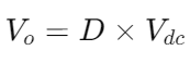 . This shows that the output voltage 𝑉𝑜Vo is directly proportional to the input voltage 𝑉𝑑𝑐, scaled by the duty cycle 𝐷, which ranges from 0 to 1.
This connection highlights the converter’s ability to control the output voltage as a specific fraction of the input voltage, dictated by the duty cycle. Understanding this principle is key to optimizing performance and developing control strategies in real-world applications.
Design and Performance Evaluation for Buck Converters
Designing a buck converter involves careful selection and rating of key components such as the inductor, switch, diode, and capacitor. This ensures the converter operates efficiently and reliably under different conditions.
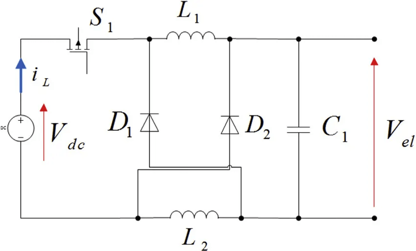
Figure 5: Inductor Design
Inductor Design for Buck Converters
The inductor's role is to store and release energy efficiently. Its design focuses on calculating the required inductance and ensuring it can handle peak currents. The analytical inductance (𝐿𝑐) is the minimum value needed to maintain continuous conduction mode (CCM) at the lowest load, preventing the inductor current from dropping to zero. The actual inductance (𝐿L) should be at least 5% higher than 𝐿𝑐 to ensure safety. This value is determined by: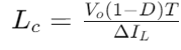 ,where 𝑉𝑜 is the output voltage, 𝐷 is the duty cycle, 𝑇 is the switching period, and Δ𝐼𝐿 is the
peak-to-peak-inductor-ripple-current. The inductor must also handle the
peak current, calculated as:
,where 𝑉𝑜 is the output voltage, 𝐷 is the duty cycle, 𝑇 is the switching period, and Δ𝐼𝐿 is the
peak-to-peak-inductor-ripple-current. The inductor must also handle the
peak current, calculated as: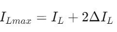 ,where IL is the average inductor current.
Figure 6: Switch Design
Switch Design in Buck Converters
The switch must handle voltages and currents higher than the maximum operating conditions. Its voltage rating should be at least 20% above the highest input voltage to handle spikes. The current rating is determined by the duty cycle and maximum output current: . This ensures the switch can manage the current without excessive heat or damage.
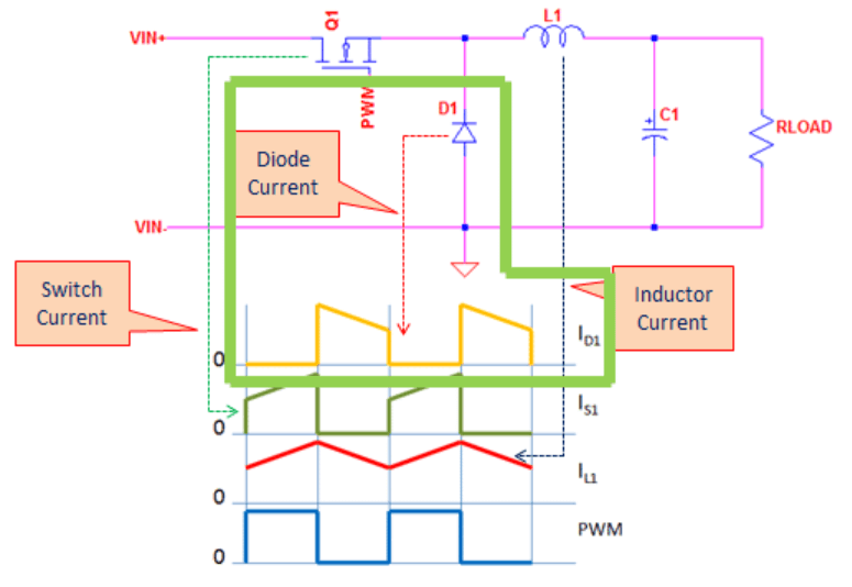
Figure 7: Diode Design
Diode Design in Buck Converters
Diodes control current flow when the switch is off. Schottky diodes are preferred for their low forward voltage drop and fast recovery time, ideal for high-frequency applications. The peak inverse voltage (𝑉𝑃𝑅𝑀) of the diode should exceed the sum of the maximum input voltage (𝑉𝐷𝐶max) and the forward voltage drop across the switch. The diode's current rating should handle the full inductor current when the switch is off: . This ensures the diode can conduct safely without overheating.
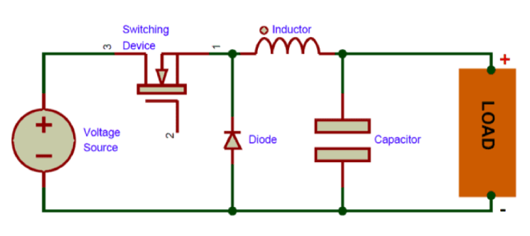
Figure 8: Capacitor Design
Capacitor Design for Buck Converters
Capacitors stabilize the output by filtering voltage ripples. Their voltage rating Vcmax must exceed the output voltage plus a margin for the expected ripple. The equivalent series resistance (ESR) of the capacitor affects voltage spike damping. The capacitance should store enough energy to respond to load or input changes, and the RMS current rating must prevent overheating: 𝐼𝑅𝑀𝑆≤Capacitor rating IRMS≤Capacitor rating. This keeps the output voltage stable within desired specifications under all conditions
Mastering Buck Converter Design
Designing a buck converter involves a step-by-step process, ensuring efficiency and functionality through precise calculations and careful parameter consideration. Follow these specific steps:
Parameter Specification: Start by defining the key parameters: input voltage, desired output voltage, and required output current. These values form the foundation for all subsequent calculations.
Duty Cycle Calculation: Calculate the duty cycle, which is key to understanding the switching properties of the converter. The duty cycle is the ratio of the output voltage to the input voltage . This ratio dictates how the converter steps down the input voltage to the desired output level.
Power Calculations
Output Power: To compute the output power Pout by multiplying the output voltage Vout by the output current Iout in code, and to consider the aspect of inefficiency between input power Pin and output power, you can use this Python code snippet:
Energy Per Pulse: For efficient high-frequency switching, calculate the energy transferred per pulse by dividing the output power by the switching frequency  .
.
Inductance Calculation
Use the energy per pulse to determine the required inductance L for efficiency and stability. Calculate inductance where 𝐸 is the energy per pulse and 𝐼 is the squared input current: . This ensures the inductor can store sufficient energy per cycle without saturation.
Choose components based on the calculations, ensuring they can handle the specified electrical conditions. Select appropriate transistors (MOSFET, IGBT, BJT), inductors, and diodes that match both the calculated values and expected real-world operational stresses.
Classification and Comparison of Buck Converter Variants
Buck converters come in two main types: non-synchronous and synchronous. Each has unique characteristics, advantages, and design complexities suited to different applications.
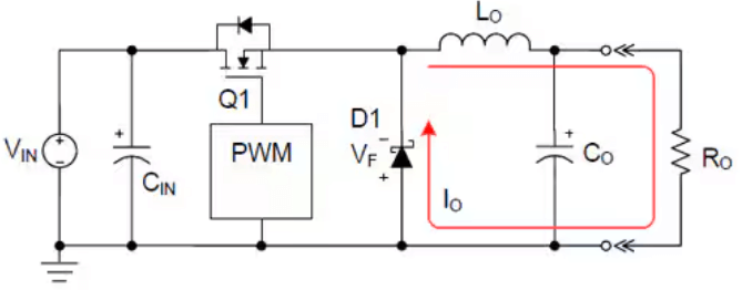
Figure 9: Non- Synchronous Variants
Non-Synchronous Buck Converters
This simpler design uses a single transistor as a switch and a diode. The transistor regulates the input voltage by intermittently allowing power to pass to the output, while the diode prevents current from flowing backward when the switch is off. Non-synchronous converters are generally less efficient due to the voltage drop across the diode during conduction, which causes power losses, especially notable in high-output current or low-output voltage applications.
in high-output current or low-output voltage applications.
Figure 10: Synchronous Variants
Synchronous Buck Converters
Synchronous converters replace the diode with a second MOSFET, acting as a synchronous rectifier, which alternates with the primary switch to reduce the voltage drop and power loss associated with diodes. This design requires precise control to manage the timing of both MOSFETs, making it imperative to avoid shoot-through, where both MOSFETs turn on simultaneously, potentially causing short circuits and serious damage. Advanced gate driving circuits and precise timing mechanisms are used to synchronize the switches safely and efficiently.
Continuous vs. Discontinuous in Buck Converter
Buck converters operate in two main conduction modes: Continuous Conduction Mode (CCM) and Discontinuous Conduction Mode (DCM). Each mode affects converter performance differently, impacting efficiency and electromagnetic compatibility.
Continuous Conduction Mode (CCM)
In CCM, the inductor current never drops to zero during the switching cycle. This mode is achieved by ensuring the inductor current stays above zero before the next cycle starts.
• Advantages
Lower Voltage Ripple: The inductor current remains continuous, resulting in a more stable output voltage with lower ripple. Applications that need exact voltages depend on this stability
Reduced Stress on Components: Constant current flow minimizes peak stresses on components, enhancing their reliability and lifespan.
For high-current applications or situations where voltage stability matters and load changes are small, like in communication equipment and precision digital devices, CCM is perfect.
Discontinuous Conduction Mode (DCM)
In DCM, the inductor current drops to zero at some point during the switching cycle before the next cycle begins. This mode usually occurs at lighter loads.
• Advantages
Higher Efficiency at Light Loads: DCM can be more efficient under light load conditions as the energy in the inductor is fully utilized each cycle, reducing losses from maintaining continuous current.
Simpler Control: Managing the buck converter can be simpler in DCM since the zero-current condition naturally resets the inductor current, aiding in switch control.
• Challenges
Higher Voltage Ripple: The intermittent current flow can lead to increased voltage ripple, which may be detrimental in sensitive applications.
Increased Electromagnetic Interference (EMI): The abrupt starting and stopping of current can generate significant electromagnetic disturbances, potentially affecting nearby electronics.
The choice between CCM and DCM depends on application demands related to efficiency, load variability, and required voltage stability. DCM is appropriate for energy conservation in systems with highly variable or discontinuous low loads, but CCM is recommended for applications where output voltage stability is needed.
Strategic Component Selection for Optimal Buck Converter Performance
The effectiveness and performance of a buck converter depend on the selection of the proper parts. Each component must be selected based on its specific role and impact on the converter’s overall functionality and reliability.
High-Side Switch
For simpler or space-constrained designs, a P-channel MOSFET is often preferred due to its easy gate driving requirements. The gate of a P-channel MOSFET can be driven directly from a supply voltage lower than the source voltage, eliminating the need for extra components.
An N-channel MOSFET, while offering better performance with lower on-resistance and higher efficiency, requires a more complex driving mechanism. To obtain the required gate voltage, a bootstrapped gate driver is typically used, resulting in the circuit design more complex. However, in high-performance applications where efficiency is harsh, this complexity may be valuable.
Diode
In order to transfer power accurately and reduce losses during the "off" part of the switching cycle, the diode is needed. A Schottky diode is highly recommended because of its low forward voltage drop and fast switching capabilities. These features make it ideal for handling high currents with minimal voltage loss, thus enhancing the overall efficiency of the buck converter, especially in high-frequency applications.
Capacitor
The output capacitor value significantly affects the output voltage ripple and the stability of the converter's output. Capacitors ranging from 100µF to 680µF are typically adequate for low current applications. The exact value should be chosen based on the application's specific needs, considering factors such as the maximum allowable ripple, load current, and switching frequency.
While electrolytic capacitors are used for their high capacitance values at a low cost, ceramic capacitors are often preferred in modern designs due to their superior frequency response and reliability.
Practical Applications of Buck Converters in Modern Electronics
Buck converters' effective voltage regulation capabilities make them requisite in a wide range of technologies. A thorough examination of their uses in numerous domains is provided below.
• Consumer Electronics
Buck converters step down the higher mains voltage to lower levels required by components like processors and memory modules. This efficient power management optimizes performance and extends battery life in portable devices.
• Telecommunications
These systems need stable, low-noise power supplies to maintain communication signal integrity. Buck converters provide precise voltage levels needed by sensitive RF components, minimizing signal distortion and enhancing the reliability of telecommunications infrastructure.
• Automotive Industry
Modern vehicles, especially electric and hybrid models, use buck converters to manage power distribution within complex electronic systems. This includes infotainment modules, GPS, and engine controls. Buck converters convert high-voltage outputs from the battery to usable levels for various electronic devices, ensuring optimal performance and safety.
• Renewable Energy Systems
Buck converters optimize energy capture by adjusting the voltage output from solar panels and wind turbines to optimal levels for storage or grid transmission. The overall effectiveness and productivity of renewable energy systems must be increased, and this requires voltage tuning.
• Portable and Wearable Devices
Buck converters manage battery output to match the specific power requirements of different components within these devices. By efficiently converting and regulating voltage, they extend battery life and reduce the need for frequent recharging, which is requisite for user convenience and device longevity.
Conclusion
Buck converters stand as a basis in the field of power electronics, providing a reliable and efficient means of stepping down voltage to meet the specific needs of various electronic devices and systems. Their ability to manage and regulate power with precision is achieved through a meticulous design process involving the careful selection of components such as inductors, switches, diodes, and capacitors.
By understanding the principles of energy storage and transfer, as well as the significance of continuous and discontinuous conduction modes, we can optimize the performance of these converters for different applications. Buck converters are going to be an integral part of electronic innovation as long as we can guarantee efficient and dependable power delivery. With continued research and development, we should anticipate even higher gains in the functionality and efficiency of these fundamental parts, expanding the potential of electronic systems in all sectors of the economy.
Frequently Asked Questions [FAQ]
1. What is the buck converter design?
A buck converter is a type of power supply that efficiently converts a higher input voltage to a lower output voltage using a switch, a diode, an inductor, and a capacitor. The design typically involves selecting these components based on the desired output voltage and current requirements.
2. What is the principle of operation of Buck and Boost converters?
Buck Converter: It operates by switching the input voltage on and off rapidly with a transistor, controlling the average voltage reaching the output. When the switch is on, current flows through the inductor and the load, storing energy in the inductor. When the switch is off, the inductor releases its stored energy to the load via the diode, maintaining the output voltage.
Boost Converter: It also uses a switch, diode, inductor, and capacitor. However, its operation inverts that of the buck converter: the switch’s opening and closing build up energy in the inductor. When the switch is off, the inductor's voltage adds to the input voltage, boosting it at the output.
3. What are the basic equations for buck converter?
The primary equations governing a buck converter are:
Output Voltage (𝑉𝑜𝑢𝑡): 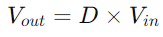 , where 𝐷 is the duty cycle of the switch (the proportion of the time it is closed).
Inductor Current Ripple (Δ𝐼𝐿) : 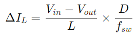 , where 𝐿 is the inductance and 𝑓𝑠𝑤 is the switching frequency.
Output Voltage Ripple (Δ𝑉𝑜𝑢𝑡):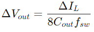 , with 𝐶𝑜𝑢𝑡 as the output capacitance.
4. Where do we use buck converter and why?
Buck converters are widely used in applications where efficiency and space are focal, such as in portable devices (smartphones, laptops), power supply modules, and any system requiring regulated lower voltage from a higher voltage source. They are chosen for their ability to efficiently step-down voltage with minimal heat generation.
5. What are the advantages and disadvantages of a buck converter?
Advantages:
High Efficiency: Can achieve efficiencies over 90%, reducing energy loss and heat.
Compact Design: Uses fewer components, enabling smaller and lighter circuit designs.
Adjustable Output Voltage: Can be fine-tuned through the duty cycle.
Disadvantages:
Complex Control: Requires precise control of the switching element to maintain stability and respond to changes in load or input voltage.
Electromagnetic Interference (EMI): Rapid switching generates noise, potentially interfering with nearby electronic devices.
Voltage Limitation: Output voltage is always lower than the input voltage, limiting its application in scenarios where an increase is required.

About us
ALLELCO LIMITED
Read more
Quick inquiry
Please send an inquiry, we will respond immediately.
Exploring DIAC Functionality in Various Application Circuits
on May 31th
Centrifugal Switch Guide - Types, Symbols, Operating Principles, and Applications
on May 30th
Popular Posts
-
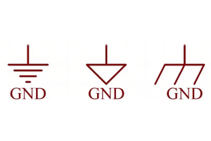
What is GND in the circuit?
on January 1th 2946
-

RJ-45 Connector Guide: RJ-45 Connector Color Codes, Wiring Schemes, R-J45 Applications, RJ-45 Datasheets
on January 1th 2502
-

Fiber Connector Types: SC Vs LC And LC Vs MTP
on January 1th 2091
-
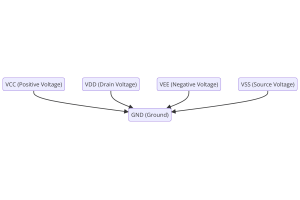
Understanding Power Supply Voltages in Electronics VCC, VDD, VEE, VSS, and GND
on November 9th 1898
-

Comparison Between DB9 and RS232
on January 1th 1765
-

What Is An LR44 Battery?
Electricity, that ubiquitous force, quietly permeates every aspect of our daily lives, from trivial gadgets to life-threatening medical equipment, it plays a silent role. However, truly grasping this energy, especially how to store and efficiently output it, is no easy task. It is against this background that this article will focus on a type of coin cell battery that may seem insignificant on the...on January 1th 1714
-
Understanding the Fundamentals:Inductance Resistance, andCapacitance
In the intricate dance of electrical engineering, a trio of fundamental elements takes center stage: inductance, resistance, and capacitance. Each bears unique traits that dictate the dynamic rhythms of electronic circuits. Here, we embark on a journey to decipher the complexities of these components, to uncover their distinct roles and practical uses within the vast electrical orchestra. Inductan...on January 1th 1662
-

CR2430 Battery Comprehensive Guide: Specifications, Applications and Comparison to CR2032 Batteries
What is CR2430 battery ?Benefits of CR2430 BatteriesNormCR2430 Battery ApplicationsCR2430 EquivalentCR2430 VS CR2032Battery CR2430 SizeWhat to look for when buying the CR2430 and equivalentsData Sheet PDFFrequently Asked Questions Batteries are the heart of small electronic devices. Among the many types available, coin cells play a crucial role, commonly found in calculators, remote controls, and ...on January 1th 1567
-
What Is RF and Why Do We Use It?
Radio Frequency (RF) technology is a key part of modern wireless communication, enabling data transmission over long distances without physical connections. This article delves into the basics of RF, explaining how electromagnetic radiation (EMR) makes RF communication possible. We will explore the principles of EMR, the creation and control of RF signals, and their wide-ranging uses. The article ...on January 1th 1550
-

CR2450 vs CR2032: Can The Battery Be Used Instead?
Lithium manganese batteries do have some similarities with other lithium batteries. High energy density and long service life are the characteristics they have in common. This kind of battery has won the trust and favor of many consumers because of its unique safety. Expensive tech gadgets? Small appliances in our homes? Look around and you'll see them everywhere. Among these many lithium-manganes...on January 1th 1519
HOT Part Number
-

C157M
Powerex Inc.
SCR 600V 110A TO83
12063G104ZAT4A
KYOCERA AVX
CAP CER 0.1UF 25V Y5V 1206
1N4448W-TP
Micro Commercial Co
DIODE GEN PURP 75V 250MA SOD123
TLC5954RTQT
Texas Instruments
IC LED DRV LIN 24.4/34.9MA 56QFN
MCC56-14IO1B
IXYS
MOD THYRISTOR DUAL 1400V TO240AA
0297020.WXNV
Littelfuse Inc.
FUSE AUTO 20A 32VDC BLADE MINI
FWH-500A
Eaton - Bussmann Electrical Division
FUSE CARTRIDGE 500A 500VAC/VDC
XC6221A2427R-G
Torex Semiconductor Ltd
IC REG LINEAR 2.4V 200MA 4USPN
USB2514B-AEZC-TR
Microchip Technology
IC CONTROLLER USB 36QFN
MBRB3030CT
onsemi
DIODE ARRAY SCHOTTKY 30V D2PAK
PS1101WA-24-TR
Stanley Electric Co
LED INDICATION SMD
AP2822CKETR-G1
Diodes Incorporated
IC PWR SWITCH N-CHAN 1:1 SOT23-5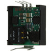
PT78NR252H
Texas Instruments
DC DC CONVERTER -5.2V 2A
04023C101JAT2A
KYOCERA AVX
CAP CER 100PF 25V X7R 0402
ICS95VLP857AKLF
Renesas Electronics America Inc
IC CLK BUF DDR 233MHZ 1CIRC
KSZ9131RNXI-TR
Microchip Technology
IC TXRX FULL/HALF 4/4 48QFN
BD3181FVM-TR
Rohm Semiconductor
IC CURRENT SENSE 1 CIRCUIT 8MSOP
74ACT10PC
onsemi
IC GATE NAND 3CH 3-INP 14DIP -

FOD073LR1
onsemi
OPTOISOLTR 2.5KV 2CH DARL 8SOIC
1808GC102KAT2A
KYOCERA AVX
CAP CER 1000PF 2KV X7R 1808
TPSE477K006R0060
KYOCERA AVX
CAP TANT 470UF 10% 6.3V 2917
STTH2R06RL
STMicroelectronics
DIODE GEN PURP 600V 2A DO41
SN74LVC3G34DCUT
Texas Instruments
IC BUFFER NON-INVERT 5.5V 8VSSOP
S25FL128SAGBHI310
Infineon Technologies
IC FLASH 128MBIT SPI/QUAD 24BGA
PVT212PBF
Infineon Technologies
SSR RELAY SPST-NO 550MA 0-150V
LT8650SEV#PBF
Analog Devices Inc.
IC REG BCK 3.3V/5V 4A DL 32LQFN
GRM1885C2A220JA01D
Murata Electronics
CAP CER 22PF 100V C0G/NP0 0603
RP118K311D-TR
Nisshinbo Micro Devices Inc.
IC REG LIN 3.1V 100MA DFN1010-4
NCP303LSN10T1G
onsemi
IC SUPERVISOR 1 CHANNEL 5TSOP
RT1206DRE0724R9L
YAGEO
RES SMD 24.9 OHM 0.5% 1/4W 1206
MCP1804T-5002I/DB
Microchip Technology
IC REG LINEAR 5V 150MA SOT223-3
NTB5405NG
onsemi
MOSFET N-CH 40V 116A D2PAK
LTC1290BCSW#TRPBF
Analog Devices Inc.
IC DAS/ADC 12BIT 50K 20SOIC
MCR03EZPFX2703
Rohm Semiconductor
RES SMD 270K OHM 1% 1/10W 0603
BSC029N025SG
Infineon Technologies
N-CHANNEL POWER MOSFET
MSC7116VM1000
NXP USA Inc.
DSP 16BIT W/DDR CTRLR 400-MAPBGA -

TCA505BG
Infineon Technologies
IC SWITCH PROX INDCT PDSO-16
FQA70N15
Fairchild Semiconductor
POWER FIELD-EFFECT TRANSISTOR, 7
MMBFJ175
onsemi
JFET P-CH 30V SOT23-3
06031A101MAT2A
KYOCERA AVX
CAP CER 100PF 100V C0G/NP0 0603
MC78L05ABPREG
onsemi
IC REG LINEAR 5V 100MA TO92-3
AOB2500L
Alpha & Omega Semiconductor Inc.
MOSFET N-CH 150V 11.5/152A TO263
TLV1018-25YDCR
Texas Instruments
IC AMP CLASS AB MONO 4DSBGA
CL02A473KQ2NNNC
Samsung Electro-Mechanics
CAP CER 0.047UF 6.3V X5R 01005
ATF1500A-15JC
Microchip Technology
IC CPLD 32MC 15NS 44PLCC
C3216CH1H562K060AA
TDK Corporation
CAP CER 5600PF 50V CH 1206
MLG0603P2N4CT000
TDK Corporation
FIXED IND 2.4NH 500MA 200MOHM SM
1N3268R
Microchip Technology
STANDARD RECTIFIER
MC74HCT273ADWG
onsemi
IC FF D-TYPE SNGL 8BIT 20SOIC
MC74HC86AFELG
onsemi
IC GATE XOR 4CH 2-INP SOEIAJ-14
IXGH35N120C
IXYS
IGBT 1200V 70A 300W TO247AD
LT1014ACN#PBF
Analog Devices Inc.
IC OPAMP GP 4 CIRCUIT 14DIP
BZT52C47
Diotec Semiconductor
DIODE ZENER 47V 500MW SOD123F
BZT55C3V9
Taiwan Semiconductor Corporation
QMMELF, 500MW, 5%, SMALL SIGNAL