IC 7404 Comprehensive Guide - Truth Table, Uses, Pros and Cons, Applications, Pinouts
Catalog
1. 7404 Integrated Circuit Description
2. Characteristics and Parameter Specifications of IC 7404
2.1 Features:
- - Six inverted outputs: The 7404 IC has six inverters in one package, making it highly effective for complex circuits that require multiple inversions simultaneously.
- - Compatible output connections: The IC's outputs are compatible with CMOS, NMOS, and TTL logic families, enabling easy integration into various digital systems, thereby reducing complexity and enhancing reliability.
- - Multiple operating voltage ranges: It supports a wide range of operating voltages, allowing it to adapt to different power supplies and enhancing its application flexibility.
- - Broad operating conditions: The IC is optimized for various environmental conditions, providing the reliability and stability necessary for industrial and commercial applications.
2.2 Parameter Specifications:
- - Maximum current output: 8mA
- - Power supply voltage range: +4.75V to +5.25V
- - Operating temperature range: -70°C to +70°C
- - Maximum supply voltage: +7V
- - Maximum rise time: 15ns
- - Maximum fall time: 15ns
- - Output type: TTL
- - Logic type: Bipolar
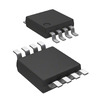
3. IC 7404 Pin Configuration and Layout
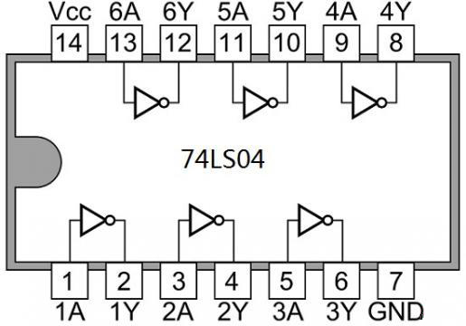
- - Pin 1, A input for gate 1
- - Pin 2, Y output for gate 1
- - Pin 3, A input for gate 2
- - Pin 4, Y output for gate 2
- - Pin 5, A input for gate 3
- - Pin 6, Y output for gate 3
- - Pin 7, Ground
- - Pin 8, Y output for gate 4
- - Pin 9, A input for gate 4
- - Pin 10, Y output for gate 5
- - Pin 11, A input for gate 5
- - Pin 12, Y output for gate 6
- - Pin 13, A input for gate 6
- - Pin 14, Positive power supply
4. 7404 IC Truth Table
|
importation(A) |
exports(Y) |
|
0 |
1 |
|
1 |
0 |
5. Functionality of the IC 7404
5.1 Inverter Operation
1. Input Signal Reception: Each inverter receives an individual input signal, which can exist in one of two states: high or low.
2. Signal Inversion Process: Upon receiving the signal, the inverter activates its logic mechanism to invert the state of the signal:
- - If the input is high (logical level 1), the output becomes low (logical level 0).
- - If the input is low (logical level 0), the output switches to high (logical level 1).
5.2 Utility in Logic Circuits
- - Building Complex Operations: By combining multiple NOT gates, complex logical functions required for advanced electronic systems can be built.
- - Multifunctional Applications: They are crucial for generating precise control and timing needed to manage various digital operations, from simple timing circuits to more complex computational logics.
5.3 Integration of Six Independent Inverters
- - Independent Operation: Each inverter operates autonomously, allowing multiple inversion operations simultaneously without interference.
- - Simplified Design and Assembly: By integrating multiple gates into one unit, the 7404 IC reduces the complexity and number of components needed on the circuit board, simplifying the design and speeding up the assembly process.
6. Advantages and Disadvantages of IC 7404
|
Advantages |
Disadvantages |
|
low power |
Limit output current |
|
high noise immunity |
Voltage range limitation |
|
user-friendly |
Not suitable for high speed applications |
|
inexpensive |
|
7. Equivalents of IC 7404
- - Pin Compatibility: Ensuring pin compatibility is crucial for seamless replacement when using an equivalent product.
- - Voltage and Current Ratings: Check the voltage and current ratings to confirm that the replacement part can meet the specific requirements of the circuit.
- - Additional Features: Depending on the application, consider whether additional features (such as the Schmitt trigger inputs in the 74LS14) may be beneficial.
8. Applications of IC 7404
- - General logic
- - Servers
- - Memory units
- - Personal computers and laptops
- - Digital Electronics
- - Networking
- - Digital systems
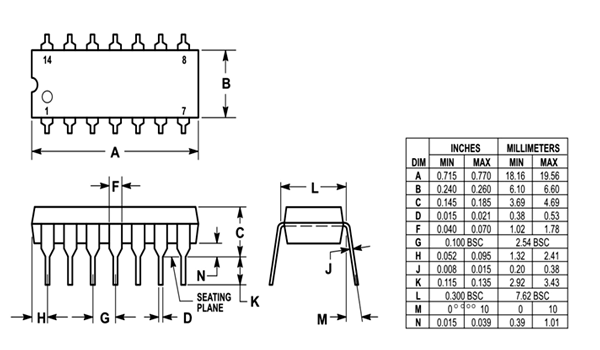
9. IC 7404 2D Packaging Model
10. IC 7404 Datasheet
Frequently Asked Questions [FAQ]
1. Is 7404 logic NOT gate or inverter?
2. Why is TTL better than CMOS?
3. How do I know if my IC is TTL or CMOS?
About us
ALLELCO LIMITED
Read more
Quick inquiry
Please send an inquiry, we will respond immediately.
Silver Oxide Batteries and Alkaline Batteries: Working Principle, Characteristics and Differences
on April 24th
AG10 Battery and Equivalent Battery Replacement
on April 23th
Popular Posts
-
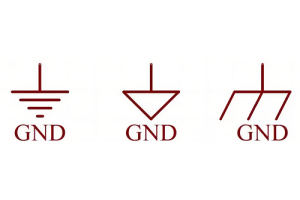
What is GND in the circuit?
on January 1th 3251
-

RJ-45 Connector Guide: RJ-45 Connector Color Codes, Wiring Schemes, R-J45 Applications, RJ-45 Datasheets
on January 1th 2801
-
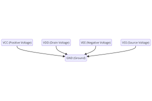
Understanding Power Supply Voltages in Electronics VCC, VDD, VEE, VSS, and GND
on November 19th 2605
-

Fiber Connector Types: SC Vs LC And LC Vs MTP
on January 1th 2249
-

Comparison Between DB9 and RS232
on January 1th 1867
-

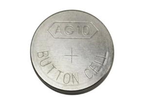
What Is An LR44 Battery?
Electricity, that ubiquitous force, quietly permeates every aspect of our daily lives, from trivial gadgets to life-threatening medical equipment, it plays a silent role. However, truly grasping this energy, especially how to store and efficiently output it, is no easy task. It is against this background that this article will focus on a type of coin cell battery that may seem insignificant on the...on January 1th 1836
-
Understanding the Fundamentals:Inductance Resistance, andCapacitance
In the intricate dance of electrical engineering, a trio of fundamental elements takes center stage: inductance, resistance, and capacitance. Each bears unique traits that dictate the dynamic rhythms of electronic circuits. Here, we embark on a journey to decipher the complexities of these components, to uncover their distinct roles and practical uses within the vast electrical orchestra. Inductan...on January 1th 1789
-
What Is RF and Why Do We Use It?
Radio Frequency (RF) technology is a key part of modern wireless communication, enabling data transmission over long distances without physical connections. This article delves into the basics of RF, explaining how electromagnetic radiation (EMR) makes RF communication possible. We will explore the principles of EMR, the creation and control of RF signals, and their wide-ranging uses. The article ...on January 1th 1779
-
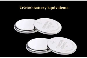
CR2430 Battery Comprehensive Guide: Specifications, Applications and Comparison to CR2032 Batteries
What is CR2430 battery ?Benefits of CR2430 BatteriesNormCR2430 Battery ApplicationsCR2430 EquivalentCR2430 VS CR2032Battery CR2430 SizeWhat to look for when buying the CR2430 and equivalentsData Sheet PDFFrequently Asked Questions Batteries are the heart of small electronic devices. Among the many types available, coin cells play a crucial role, commonly found in calculators, remote controls, and ...on January 1th 1775
-
Comprehensive guide to hFE in transistors
Transistors are crucial components in modern electronic devices, enabling signal amplification and control. This article delves into the knowledge surrounding hFE, including how to select a transistor's hFE value, how to find hFE, and the gain of different types of transistors. Through our exploration of hFE, we gain a deeper understanding of how transistors work and their role in electronic circu...on November 19th 1760
HOT Part Number
-
04025C332JAT2A
AVX Corporation
CAP CER 3300PF 50V X7R 0402
08051A1R5BAT2A
AVX Corporation
CAP CER 1.5PF 100V C0G/NP0 0805
AS1744G-T
ams OSRAM
IC SWITCH SPDT X 2 4OHM 10MSOP
GRM2196T2A9R5DD01D
Murata Electronics
CAP CER 9.5PF 100V T2H 0805
08051U910FAT9A
KYOCERA AVX
CAP CER 91PF 100V C0G/NP0 0805
PJSD36CW_R1_00001
Panjit International Inc.
SOD-323, TVS/ESD
SMAJ20A
Bourns Inc.
TVS DIODE 20VWM 32.4VC SMA
GR455DR73D103KW01L
Murata Electronics
CAP CER 10000PF 2KV X7R 2220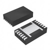
BQ27411DRZR-G1C
Texas Instruments
IC BATT FUEL GAUGE LICOO2 12SON
KT11S2SA2M34LFS
C&K
SWITCH TACTILE SPST-NO 1VA 32V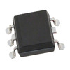
PC3SD11NXZCF
Sharp Microelectronics
OPTOISOLATOR 5KV TRIAC 6SMD
TPS79518DCQRG4
Texas Instruments
IC REG LIN 1.8V 500MA SOT223-6
OHD5R-115B
KEMET
THERMOSTAT 115DEG C SPST-NC MOD
VI-27Y-EX
Vicor Corporation
DC DC CONVERTER 3.3V 15W
C0805C150J5GACTU
KEMET
CAP CER 15PF 50V C0G/NP0 0805
RT0603DRE07470RL
YAGEO
RES SMD 470 OHM 0.5% 1/10W 0603
MTFC64GAJAECE-AIT
Micron Technology Inc.
IC FLASH 512GBIT MMC 169LFBGA
LQW18AN22NG00D
Murata Electronics
FIXED IND 22NH 500MA 170MOHM SMD -
MAX7410EUA+T
Analog Devices Inc./Maxim Integrated
IC FILTER 15KHZ BUTTER 8UMAX
MBD54DWT1
onsemi
DIODE SCHOTTKY DUAL 30V SOT363
HUF76639S3ST
onsemi
MOSFET N-CH 100V 51A D2PAK
2N3635
Microchip Technology
TRANS PNP 140V 1A TO39
ISL9N310AD3ST
Fairchild Semiconductor
N-CHANNEL POWER MOSFET
KSD1273PTU
onsemi
TRANS NPN 60V 3A TO220F-3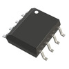
LTC1153IS8#PBF
Analog Devices Inc.
IC ELECTR CIRCUIT BREAKER 8-SOIC
GRM188R71H272KA01D
Murata Electronics
CAP CER 2700PF 50V X7R 0603
170M4696
Eaton - Bussmann Electrical Division
FUSE SQUARE 550A 1.3KVAC RECT
1812GA221JAT3A
KYOCERA AVX
CAP CER 220PF 2KV C0G/NP0 1812
1-66105-9
TE Connectivity AMP Connectors
CONN SOCKET 20-24AWG TIN CRIMP
AD774BJN
Analog Devices Inc.
IC ADC 12BIT SAR 28DIP
IHLP2525CZER1R5M07
Vishay Dale
FIXED IND 1.5UH 9A 14.5 MOHM SMD
V72C28C150BL
Vicor Corporation
DC DC CONVERTER 28V 150W
MMBF4119
onsemi
JFET N-CH 40V SOT23-3
KA7906TU
onsemi
IC REG LINEAR -6V 1A TO220-3
DRA5124E0L
Panasonic Electronic Components
TRANS PREBIAS PNP 150MW SMINI3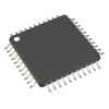
PIC32MX250F128DT-I/PT
Microchip Technology
IC MCU 32BIT 128KB FLASH 44TQFP -

LT6604IUFF-2.5#PBF
Analog Devices Inc.
IC OPAMP DIFF 2 CIRCUIT 34QFN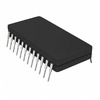
AD698SQ
Analog Devices Inc.
IC LVDT SGNL COND UNVRSL 24CDIP
AD7276BUJZ-REEL7
Analog Devices Inc.
IC ADC 12BIT SAR TSOT23-6
NUF4107FCT1G
onsemi
FILTER RC(PI) 100 OHM/60PF SMD
MAC16NG
Littelfuse Inc.
TRIAC 800V 16A TO220AB
BZG05C5V6-E3-TR
Vishay General Semiconductor - Diodes Division
DIODE ZENER 5.6V 1.25W DO214AC
DTC643TUT106
Rohm Semiconductor
TRANS PREBIAS NPN 200MW UMT3
TAJB105K035RNJ
KYOCERA AVX
CAP TANT 1UF 10% 35V 1411
GRM55DR72E684KW01L
Murata Electronics
CAP CER 0.68UF 250V X7R 2220
VI-J6L-MY
Vicor Corporation
DC DC CONVERTER 28V 50W
MAX6894ETI+T
Analog Devices Inc./Maxim Integrated
IC SUPERVISOR 4 CHANNEL 28TQFN
NAND512W3A2SNXE
Micron Technology Inc.
IC FLASH 512MBIT PAR 48TSOP I
INA145UA/2K5
Texas Instruments
IC OPAMP DIFF 1 CIRCUIT 8SOIC
RT0805BRD0718KL
YAGEO
RES SMD 18K OHM 0.1% 1/8W 0805
EPF8452AGC160-3
Altera
LOADABLE PLD, CMOS, CPGA160
C2012C0G2A471J
TDK Corporation
CAP CER 470PF 100V C0G 0805
1N2136
Solid State Inc.
DIODE GEN PURP 450V 70A DO5
74AUP1G02FX4-7
Diodes Incorporated
IC GATE NOR 1CH 2-INP DFN1409-6