Exploring Piezoelectric Materials: Types, Properties, and Technological Impact
Over the years, advances in material science have created different piezoelectric materials such as single crystals, ceramics, and thin films. This article takes a close look at piezoelectric materials including their properties, types, how they work, and their uses. It highlights their importance in linking mechanical and electrical engineering, driving innovation in many areas.
Catalog
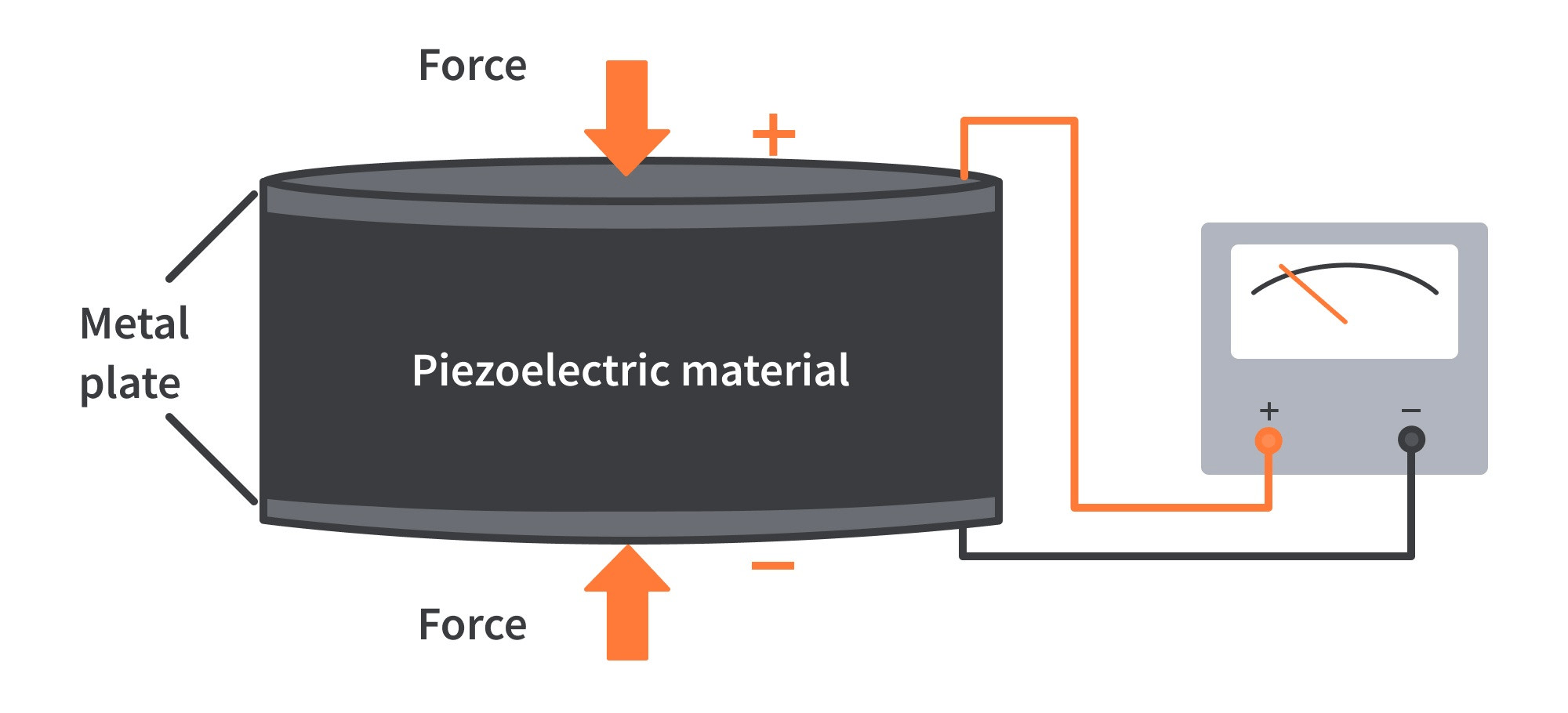
Figure 1: Piezoelectric Material
What Is Piezo?
The word "piezo" comes from the Greek word "piezein," means "to press" or "pressure." This fits well with its use in science for piezoelectricity. In 1880, French physicists Jacques and Pierre Curie discovered piezoelectricity. They found that when certain crystals like tourmaline, quartz, topaz, and Rochelle salt, were pressed, they produced an electrical charge. They also saw that these crystals could change shape when an electrical current was applied showing that the process could work both ways.
This discovery led to the creation of various piezoelectric devices. During World War I, piezoelectricity was mainly used in ultrasonic submarine detectors. Today, piezoelectric materials are used in many things. They are found in everyday items like electric cigarette lighters and inkjet printers, as well as in advanced technologies like medical ultrasound imaging and precision motion control in robotics.
Types of Piezoelectric Materials

Figure 2: Examples of Piezoelectric Materials
Single Crystal Piezoelectric Materials
Single crystal piezoelectric materials are characterized by their continuous and uniform crystal lattice, free from grain boundaries. This uniform structure often leads to better electromechanical coupling efficiencies compared to other piezoelectric materials. Examples of such materials include quartz and langasite. These single crystals are produced using precise growth methods like the Czochralski process or hydrothermal synthesis. Their exceptional performance makes them perfect for precise applications like advanced medical imaging systems, telecommunications resonators and filters, and vibration monitoring in aerospace.

Figure 3: Piezo Crystal Quartz Material
Ceramic Piezoelectric Materials
Piezoelectric ceramics are made from perovskite-structured materials like lead zirconate titanate (PZT). These materials are polycrystalline and are created by sintering powdered substances. Their piezoelectric properties are developed through a poling process and aligns the electric dipoles by applying an external electric field. These ceramics can be easily shaped into various forms and sizes. Their durability and cost-effectiveness make them popular for use in actuators, sensors, ultrasonic transducers, and consumer electronics buzzers.
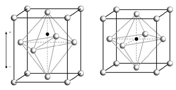
Figure 4: Structure of PZT Type Piezoelectric Ceramic
Thin Film Piezoelectric Materials
Thin film piezoelectrics are made by depositing layers that range from a few nanometers to several micrometers in thickness using advanced fabrication techniques like sputtering, chemical vapor deposition or pulsed laser deposition. Common materials used in thin films include PZT, zinc oxide (ZnO), and aluminum nitride (AlN). The thinness of these films allows them to be integrated into microelectromechanical systems (MEMS) and nanoelectromechanical systems (NEMS), enhancing their functionality in compact devices such as microphones, microswitches and advanced sensor arrays. Their compatibility with standard semiconductor processes and scalability makes them suitable for integrated circuits and flexible electronics.
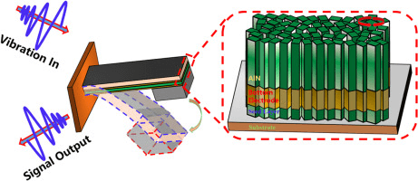
Figure 5: AlN Piezoelectric Thin Films
Figure 6: Bulk Piezo Elements
Choosing between thin-film and bulk piezoelectric materials depends on the application's specific needs for precision, power and durability. Thin-film piezo materials are suited in small-scale technologies. In contrast, bulk piezo materials are preferred in more demanding, larger-scale applications. The table below compares thin-film piezo materials and bulk piezo materials based on their thickness, manufacturing techniques, key features and applications.
|
Category |
Thin-Film Piezo Materials |
Bulk Piezo Materials |
|
Thickness |
A few nanometers to several micrometers |
Several millimeters to centimeters |
|
Manufacturing Techniques |
Sputtering, pulsed laser deposition,
chemical vapor deposition |
Pressing, extrusion, machining |
|
Features |
High-Frequency Response: Quick response
times |
High Power Generation: Produces power
under mechanical stress |
|
Flexibility: Applicable to flexible
surfaces |
Durability: Strong and durable, suitable
for heavy loads and harsh conditions |
|
|
Precision: Precise control on a
microscopic level |
Versatility: Easily shaped and sized for
specific needs |
|
|
Applications |
Microelectronics and MEMS:
Accelerometers, gyroscopes, inkjet printer heads |
Energy Harvesting: Converts mechanical
stress from vibrations into electrical energy |
|
Medical Devices: Ultrasonic transducers
for imaging and therapy |
Actuators and Sensors: Large actuators in
automotive and aerospace industries, high-load sensors |
|
|
Telecommunications: Filters and
resonators in mobile phones and communication devices |
Sonar and Ultrasonic Devices: Sonar
systems for naval use, industrial ultrasonic cleaners |
Thin-Film PZT and Deposition Methods
Thin-film lead zirconate titanate (PZT) materials are used in sensors, actuators, and microelectromechanical systems (MEMS) because of their great piezoelectric properties. The composition and effectiveness of PZT thin films depend a lot on their deposition methods that may affect their structure, orientation, and piezoelectric performance. The three main deposition techniques: sol-gel, sputtering, and Metal Organic Chemical Vapor Deposition (MOCVD).
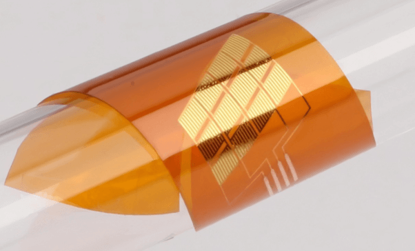
Figure 7: Flexible Thin-Film PZT
Sol-Gel Process
The sol-gel process is a cost-effective way to deposit PZT thin films and allowing control over film composition at the molecular level. This technique starts with preparing a colloidal solution (sol) that turns into a gel. Important steps include hydrolyzing and polymerizing metal alkoxides. The resulting gel is applied to a substrate using spin coating or dip-coating, followed by heat treatment to remove organic components and crystallize the PZT phase.
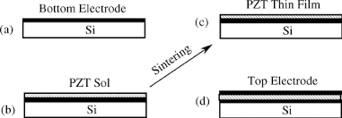
Figure 8: Sol-Gel Process for PZT Thin Films
Advantages
• Allows fine control over stoichiometry, improving piezoelectric properties
• Uses lower temperatures compared to other methods
Challenges
• It's hard to get consistent thickness and composition across large areas
• High shrinkage during drying and firing often causes cracks
Sputtering
Sputtering is a physical vapor deposition (PVD) technique where high-energy particles knock material off a target then deposits onto a substrate. For PZT films, RF magnetron sputtering is used involving a plasma of argon ions hitting the PZT target.
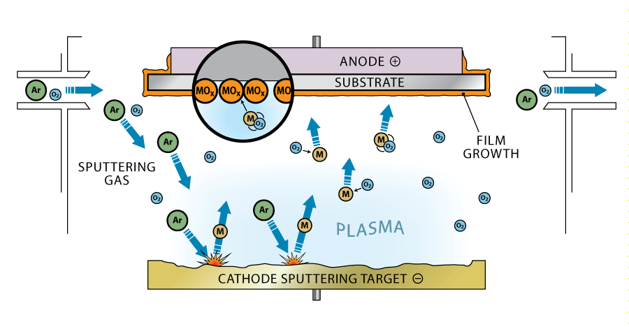
Figure 9: Sputter Deposition Method of Thin-Film Deposition
Advantages
• Produces films with good adhesion and density
• Suitable for coating large substrates uniformly
Challenges
• Stress can build up in the films affecting their properties
• The target's composition may change during sputtering due to differential sputtering yields
Metal Organic Chemical Vapor Deposition (MOCVD)
MOCVD involves decomposing metal-organic precursors in a vapor phase and react or decompose on a heated substrate to form a thin film. This method is preferred for producing high-purity, well-crystallized films suitable for electronic applications.
Advantages
• Provides excellent film uniformity and conformity even on complex-shaped substrates
• Good for high-volume production
Challenges
• Requires higher temperatures than other methods
• Handling and storage of metal-organic precursors can be hazardous
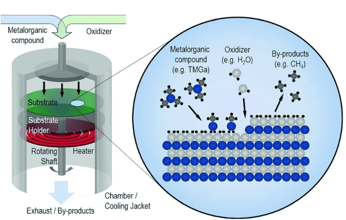
Figure 10: Metal Organic Chemical Vapor Deposition
How Materials Act Under Stress
Behavior Under Compression
When materials like quartz or barium titanate are squeezed, they change in ways that impact their use in various devices. These materials have special structures that create electrical charges when they are pressed. As they are compressed, they shrink and their internal structure changes.
This squeezing causes the electrical charges inside the crystal to become unevenly distributed. The pressure moves ions in the crystal's structure, creating an electric field. This happens because the positive and negative charge centers in the material shift. The amount of electrical response depends on the type of crystal, the force applied and the crystal's direction relative to the force.
For example, in sensors, the voltage produced by the crystals can measure the force applied making them perfect for detecting pressure and monitoring loads. In actuators, applying an electrical field can make the crystal change shape, allowing precise control of movements in things like ultrasonic devices and car fuel injectors.
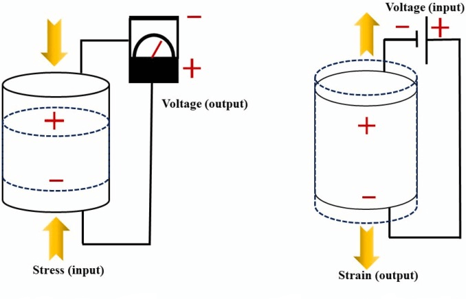
Figure 11: Piezoelectric Materials Works
Piezoelectric Response to Pressure
When piezoelectric materials face mechanical pressure, their molecules realign, affecting their electrical properties. The force changes the molecular structure, aligning regions with uniform electrical direction, increases electrical polarization.
This alignment boosts the charge separation in the material, enhancing its electrical polarization. In simple terms, the pressure makes the dipoles (molecules with two opposite charges) more uniform, creating a stronger electric field for a given force.
The ability to control this response accurately under different pressures makes piezoelectric materials very useful in many technologies. Their capability to convert mechanical pressure into electrical signals and vice versa allows them to be used effectively in tasks like generating precise electronic frequencies and monitoring vibrations in industrial settings.
The Piezoelectric Effect
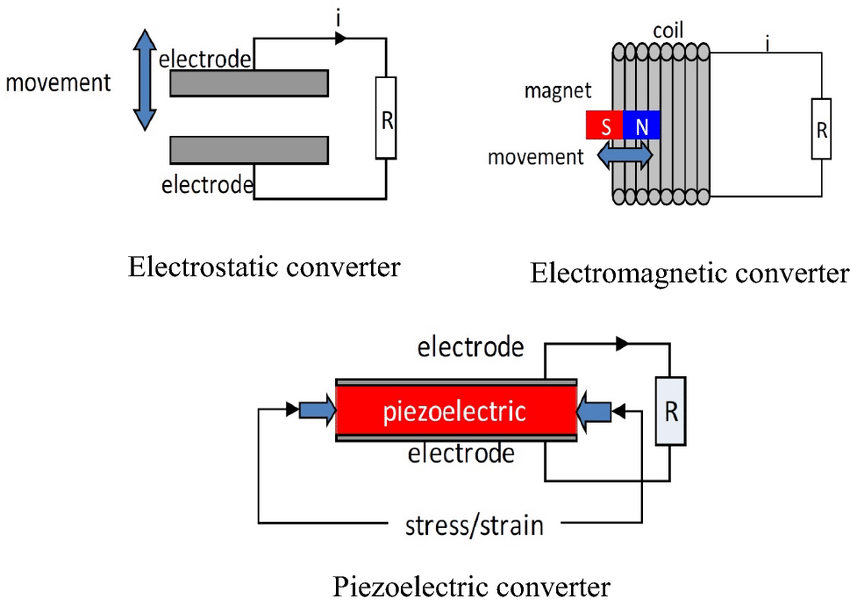
Figure 12: The Piezoelectric Effect
Turning Mechanical Energy into Electrical Energy with the Piezoelectric Effect
The piezoelectric effect changes mechanical energy into electrical energy by deforming certain crystal materials. These materials, known as piezoelectrics include natural substances like quartz and synthetic ones like advanced ceramics.
When a piezoelectric material faces mechanical stress such as being squeezed, twisted, or bent, its crystal structure, doesn't have a central symmetry and gets disturbed. This disturbance shifts the charge centers in the crystal causing polarization and creating an electrical potential at certain points in the material.
Key points of this process:
The electrical charge produced matches the amount of mechanical stress applied. This means the electrical output can be precisely controlled based on the known force applied;
When the force is removed, the material returns to its original state and the electrical charge goes away. This ensures the material's durability and reliability good for devices that need to work well repeatedly.
Turning Electrical Energy into Mechanical Energy with the Reverse Piezoelectric Effect
The reverse piezoelectric effect changes electrical energy back into mechanical energy. Applying an electrical voltage to a piezoelectric material creates an electric field that changes the crystal lattice structure, altering the material's dimensions.
This effect is used in precision actuators in optical instruments and micro-positioning systems. The reverse piezoelectric effect ensures that small electrical inputs result in precise, controlled mechanical adjustments, helping advancements in robotics, automotive technology, medical instruments, and telecommunications.
The dual ability of the piezoelectric effect to act as both a mechanical-to-electrical and electrical-to-mechanical transducer supports technological advancements. It connects the mechanical and electrical domains, expanding modern engineering and innovation.
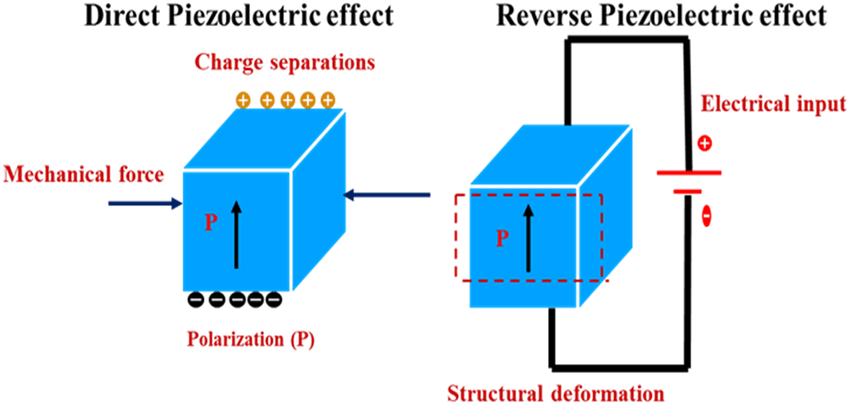
Figure 13: Direct and Reverse Piezoelectric Effect
Comparing Non-Piezoelectric and Piezoelectric Materials
Non-piezoelectric and piezoelectric materials are different in how they handle mechanical and electrical energy. Non-piezoelectric materials like steel and aluminum can conduct electricity but don't create an electric charge when stressed. Piezoelectric materials, such as quartz and certain ceramics, can change mechanical energy into electrical energy because of their special crystal structure.
Non-piezoelectric materials have symmetrical crystal lattices, so they don't produce an electric dipole when stressed. Piezoelectric materials have asymmetrical crystal lattices, that allows them to generate an electric charge when under stress. This deformation causes internal polarization and creating electrical potential.
Non-piezoelectric materials behave like regular conductors or insulators based on their electron mobility and band structure and they don't create an electric charge when deformed. Piezoelectric materials exhibit two effects: the direct piezoelectric effect, where mechanical stress generates an electric charge, and the inverse piezoelectric effect, where an electric field causes mechanical deformation. These characteristics make piezoelectric materials suitable for use in sensors and actuators.
Due to their different properties, non-piezoelectric and piezoelectric materials are used in different applications. Non-piezoelectric materials are used in structural components, electrical wiring, and standard electronic parts where strength and conductivity are important. Piezoelectric materials are utilized in fields that require precise control and mechanical-electrical energy conversion, such as ultrasound equipment, precision positioning devices, and various sensors and actuators good for advanced technologies.
Applications of Piezoelectricity
Consumer Electronics: In smartphones and other devices, piezoelectric parts are used in speakers and microphones. They turn electrical signals into sound vibrations or sound vibrations into electrical signals for audio input.
Automotive Industry: Modern cars use piezoelectric sensors for many purposes like controlling the fuel injection in engines and monitoring tire pressure.
Environmental Monitoring: Piezoelectric sensors detect pressure changes, vibrations, and sounds. They are used for checking environmental conditions and ensuring the safety of buildings and bridges.
Energy Harvesting: Piezoelectric materials can capture energy from mechanical stress. For example, floors that convert footsteps into electrical energy can power lights and electronics in busy areas, helping create sustainable environments.
High-Voltage Piezoelectric Lighters: These lighters used for lighting gas stoves and barbecues and create a high voltage from a small mechanical click, producing a spark to light the burner. This shows the practical use of piezoelectric materials.
Medical Imaging: Piezoelectric crystals are useful in ultrasound machines. They produce sound waves that bounce off tissues and organs, creating images for diagnosis.
Precision Actuators in Scientific Instruments: Piezoelectric materials in precision actuators create tiny movements for optics and nanotechnology. These actuators adjust mirrors, lenses, and other parts with microscopic accuracy for scientific research and semiconductor manufacturing.
Conclusion
Studying piezoelectric materials shows a strong connection between physics and engineering, demonstrating how their natural properties can be used for many technological purposes. The versatility of piezoelectric materials available as both strong bulk materials and flexible thin films, makes them suitable for various applications, such as energy harvesting, environmental monitoring, and developing sustainable technologies. As innovation continues, research and development in piezoelectric materials are more important, promising improvements in efficiency, precision, and functionality for future technologies.
Frequently Asked Questions [FAQ]
1. What causes electricity to be produced from piezoelectric effect?
The piezoelectric effect occurs when certain materials produce an electric charge in response to mechanical stress. These materials, a crystals like quartz, ceramics like barium titanate and some polymers, possess a crystal lattice structure that is non-centrosymmetric, meaning it lacks a center of symmetry. When mechanical force such as pressure or vibration is applied, this structure becomes distorted. This distortion displaces the ions within the lattice, creating areas with positive and negative charges. The spatial separation of these charges results in an electric potential generating electricity. This effect is reversible and applying an electric field to these materials will also induce mechanical stress.
2. What device uses the piezoelectric effect?
Devices that utilize the piezoelectric effect are varied and include both everyday and specialized equipment. Common applications are:
Quartz watches: Using the regular vibrations of quartz under an electric field to keep time accurately.
Medical ultrasound devices: Generating sound waves that echo inside the body to create diagnostic images.
Fuel injectors in cars: Using piezoelectric actuators to control the timing and amount of fuel injected into the engine cylinders.
Piezoelectric sensors and accelerometers: Measuring changes in pressure, acceleration, strain, or force by converting them into an electrical signal.
3. How many volts is a piezo?
The voltage output of a piezoelectric element can vary widely depending on its size, material, and the amount of mechanical stress applied. A small piezo element like those found in lighters or electronic devices can produce a voltage spike ranging from a few volts to several hundred volts. However, these outputs are generally at very low currents and last only microseconds.
4. Does a piezo need a resistor?
In many applications, a resistor is used with a piezoelectric element to limit the current and protect other components in the circuit from the high voltage spike produced when the piezo is activated. The value of the resistor depends on the specific requirements of the circuit including the desired response time and sensitivity. Without a resistor, the piezo can potentially damage connected electronic components due to the high initial voltage spike.
5. How is piezoelectric related to human power?
The piezoelectric effect is directly applicable to harnessing human power in innovative ways. It can convert mechanical energy from human activities, such as walking or pressing buttons, into electrical energy. This technology is explored in various applications:
Energy-harvesting floor tiles: These tiles generate electricity from the pressure of footfalls in busy areas like subway stations or malls.
Wearable technology: Embedding piezoelectric materials in shoes or clothing to generate power for small devices through normal body movements.
Medical implants: Using body movements to power devices like pacemakers, reducing or eliminating the need for external batteries.
About us
ALLELCO LIMITED
Read more
Quick inquiry
Please send an inquiry, we will respond immediately.
Comprehensive Guide to Wrist Watch Battery Replacement
on July 26th

D Battery Vs. C Battery
on July 26th
Popular Posts
-
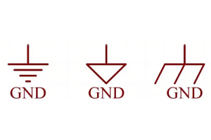
What is GND in the circuit?
on January 1th 3173
-

RJ-45 Connector Guide: RJ-45 Connector Color Codes, Wiring Schemes, R-J45 Applications, RJ-45 Datasheets
on January 1th 2748
-
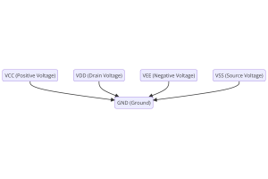
Understanding Power Supply Voltages in Electronics VCC, VDD, VEE, VSS, and GND
on November 18th 2414
-

Fiber Connector Types: SC Vs LC And LC Vs MTP
on January 1th 2216
-

Comparison Between DB9 and RS232
on January 1th 1836
-

What Is An LR44 Battery?
Electricity, that ubiquitous force, quietly permeates every aspect of our daily lives, from trivial gadgets to life-threatening medical equipment, it plays a silent role. However, truly grasping this energy, especially how to store and efficiently output it, is no easy task. It is against this background that this article will focus on a type of coin cell battery that may seem insignificant on the...on January 1th 1808
-
Understanding the Fundamentals:Inductance Resistance, andCapacitance
In the intricate dance of electrical engineering, a trio of fundamental elements takes center stage: inductance, resistance, and capacitance. Each bears unique traits that dictate the dynamic rhythms of electronic circuits. Here, we embark on a journey to decipher the complexities of these components, to uncover their distinct roles and practical uses within the vast electrical orchestra. Inductan...on January 1th 1763
-

CR2430 Battery Comprehensive Guide: Specifications, Applications and Comparison to CR2032 Batteries
What is CR2430 battery ?Benefits of CR2430 BatteriesNormCR2430 Battery ApplicationsCR2430 EquivalentCR2430 VS CR2032Battery CR2430 SizeWhat to look for when buying the CR2430 and equivalentsData Sheet PDFFrequently Asked Questions Batteries are the heart of small electronic devices. Among the many types available, coin cells play a crucial role, commonly found in calculators, remote controls, and ...on January 1th 1733
-
What Is RF and Why Do We Use It?
Radio Frequency (RF) technology is a key part of modern wireless communication, enabling data transmission over long distances without physical connections. This article delves into the basics of RF, explaining how electromagnetic radiation (EMR) makes RF communication possible. We will explore the principles of EMR, the creation and control of RF signals, and their wide-ranging uses. The article ...on January 1th 1724
-
Comprehensive guide to hFE in transistors
Transistors are crucial components in modern electronic devices, enabling signal amplification and control. This article delves into the knowledge surrounding hFE, including how to select a transistor's hFE value, how to find hFE, and the gain of different types of transistors. Through our exploration of hFE, we gain a deeper understanding of how transistors work and their role in electronic circu...on November 18th 1706
HOT Part Number
-

NCT5568D
Nuvoton Technology Corporation
IC INTERFACE SPECIALIZED
RBS80670XX
Powerex Inc.
DIODE GEN PURP 600V 7000A
MC74LVX259DTR2G
onsemi
IC LATCH ADDRESSABL 8BIT 16TSSOP
GRM1885C2A3R6CZ01D
Murata Electronics
CAP CER 3.6PF 100V C0G/NP0 0603
TMCMB0J476MTRF
Vishay Sprague
CAP TANT 47UF 20% 6.3V 1411
B3SN-3012P
Omron Electronics Inc-EMC Div
SWITCH TACTILE SPST-NO 0.05A 24V
NB4N121KMNR2G
onsemi
IC CLK BUFFER 1:21 400MHZ 52QFN
LM2737MTCX
Texas Instruments
IC REG CTRLR BUCK 14TSSOP
AT17LV512-10JU
Microchip Technology
IC SRL CONFG EEPROM 512K 20-PLCC
EP1AGX90EF1152I6N
Intel
IC FPGA 538 I/O 1152FBGA
LT3756EUD#TRPBF
Analog Devices Inc.
IC LED DRIVER CTRLR PWM 16QFN
XC5VSX50T-2FF665I
AMD
IC FPGA 360 I/O 665FCBGA
853S011CMILF
Renesas Electronics America Inc
IC CLK BUFFER 1:2 2.5GHZ 8SOIC
C1210C156K8PAC7800
KEMET
CAP CER 15UF 10V X5R 1210
LTC3814EFE-5#PBF
Analog Devices Inc.
IC REG CTRLR BOOST 16TSSOP
LMK1C1102DQFR
Texas Instruments
IC CLK BUFFER 1:2 250MHZ 8WSON
FDB9403
Fairchild Semiconductor
N-CHANNEL, MOSFET
SN74LVC139ANSR
Texas Instruments
IC DECODER/DEMUX 1 X 2:4 16SO -

LM809M3X-2.63
Texas Instruments
IC SUPERVISOR 1 CHANNEL SOT23-3
QSD2030F
Fairchild Semiconductor
PIN PHOTODIODE
2N4363
Powerex Inc.
SCR 400V 110A TO94
IS43TR16128AL-125KBLI
ISSI, Integrated Silicon Solution Inc
IC DRAM 2GBIT PARALLEL 96TWBGA
MCT6-X007T
Vishay Semiconductor Opto Division
OPTOISO 5.3KV 2CH TRANS 8SMD
MCC600-22IO1W
IXYS
MOD SCR THYRISTOR 2200V
170M6013
Eaton - Bussmann Electrical Division
FUSE SQUARE 900A 700VAC RECT
TB2600H-13-F
Diodes Incorporated
THYRISTOR 220V 400A DO214AA
CL31B224KBPWPNE
Samsung Electro-Mechanics
CAP CER 0.22UF 50V X7R 1206
TL497AID
Texas Instruments
IC REG BUCK BST ADJ 500MA 14SOIC
LT1236BIS8-5#PBF
Analog Devices Inc.
IC VREF SERIES 0.1% 8SOIC
LTC3874IUFD#PBF
Analog Devices Inc.
IC REG CTRLR BUCK 28QFN
51HQ045
Microchip Technology
DIODE SCHOTTKY 45V 60A DO5
TDA7580
STMicroelectronics
IC PROC FM/AM IF SAMPLING 64LQFP
1808SA101KAT3A
KYOCERA AVX
CAP CER 100PF 1.5KV NP0 1808
DAN222T1
onsemi
DIODE SWITCH DUAL CC 80V SC-75
C8051F920-GQ
Silicon Labs
IC MCU 8BIT 32KB FLASH 32LQFP
LTC3417EFE#PBF
Linear Technology
DUAL SYNCHRONOUS 1.4A/800MA 4MHZ -

APT8DQ60KG
Microchip Technology
DIODE GEN PURP 600V 8A TO220
MAX5915EUI
Analog Devices Inc./Maxim Integrated
DUAL PCI 2.2 HOT-SWAP CONTROLLER
F981A106MMA
KYOCERA AVX
CAP TANT 10UF 20% 10V 0603
511BCA135M000BAGR
Skyworks Solutions Inc.
XTAL OSC XO 135.0000MHZ LVDS SMD
ADS1286UL
Texas Instruments
IC ADC 12BIT SAR 8SOIC
SFF9250L
onsemi
MOSFET P-CH 200V 12.6A TO3PF
ZL30312GKG2
Microchip Technology
IC TIMING-OVER-PACKET 256TEBGA-2
UPG2409TB-E4-A
Renesas Electronics America Inc
DIVERSITY SWITCH
EFM32GG11B310F2048GQ100-B
Silicon Labs
IC MCU 32BIT 2MB FLASH 100TQFP
DTC114EETL
Rohm Semiconductor
TRANS PREBIAS NPN 150MW EMT3
STD100N3LF3
STMicroelectronics
MOSFET N-CH 30V 80A DPAK
7440700033
Würth Elektronik
FIXED IND 3.3UH 3.2A 36 MOHM SMD
PI2USB4122ZHEX
Diodes Incorporated
IC MUX/DEMUX USB DUAL 4:1
DS1672-2
Analog Devices Inc./Maxim Integrated
IC RTC BINARY COUNTER I2C 8DIP
170M7028
Eaton - Bussmann Electrical Division
FUSE SQUARE 3KA 660VAC RECT
4416P-1-100LF
Bourns Inc.
RES ARRAY 8 RES 10 OHM 16SOIC
5KP85A-E3/54
Vishay General Semiconductor - Diodes Division
TVS DIODE 85VWM 137VC P600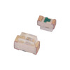
LTST-S270KFKT
Lite-On Inc.
LED ORANGE CLEAR SMD R/A