A Comprehensive Guide to DIP Packaging - History, Types, Characteristics, References
Throughout the history of electronic devices, developers have consistently prioritized the miniaturization of components. A significant breakthrough came with the effort to place several of these components on a single chip of semiconductor material, marking the beginning of the microchip era. Gradually, microcircuits—small rectangular bricks with many pins on the long side—became common components in electronic circuits. This article will explain the basics of Dual In-line Package (DIP), a common type of microcircuit. If you have any questions about DIP, you're welcome to read on.
Table of Contents
1. What is a Dual In-line Package (DIP)?
2. The History of DIP
3. Classification of DIP Structures
4. Types of DIP Chips
5. Pin Count and Spacing
6. Orientation and Pin Numbering
7. Advantages and Disadvantages of DIP
8. Characteristics of DIP
9. Applications of DIP
10. Main Differences Between DIP and SMT
1. What is a Dual In-line Package (DIP)?
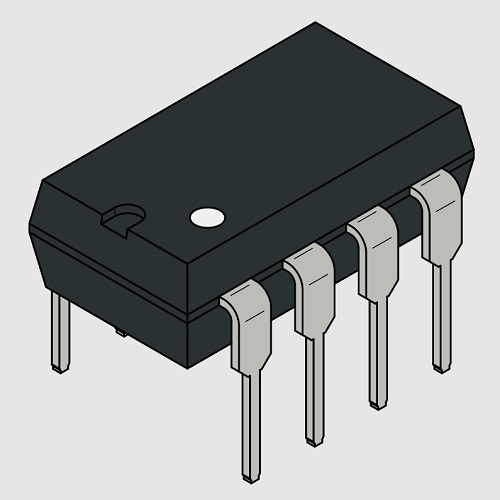
DIP package
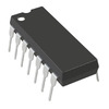
Dual In-line Package, also known as DIP packaging, is a type of integrated circuit packaging. It features a rectangular shape with two rows of parallel metal pins on either side, known as pin headers, that can be inserted into DIP sockets. The package is numbered by the total number of pins on both sides. For example, a DIP 8 chip indicates there are 8 pins, with 4 on each side. Below is an overview diagram of a DIP14 integrated circuit.
2. The History of DIP
DIP packaging was the mainstream technology from the 1970s until the emergence of surface-mount technology. This technology used a plastic case with two rows of parallel pins surrounding the semiconductor, known as the lead frame, for connection to a printed circuit board (PCB).
The actual chip was then connected to the two lead frames that could connect to a PCB via bonding wires.
Fairchild Semiconductor created DIP in 1964, marking a milestone in early semiconductor design. This packaging method became popular for its ability to seal the chip in resin, ensuring high reliability and low cost. Many early significant semiconductor products used this packaging. DIP's feature is connecting the chip to the external lead frame through wires, an application of lead bonding technology.
The Intel 8008 microprocessor is one classic example of a DIP-packaged product, representing the development of early microprocessor technology. Thus, those semiconductors resembling small spiders often used DIP packaging technology.
3. Classification of DIP Structures
- - Multilayer Ceramic Dual In-line DIP
- - Single-layer Ceramic Dual In-line DIP
- - Lead Frame DIP (including Microglass Sealed Type, Plastic Sealed Structure, Ceramic Low Melting Glass Packaging Type)
4. Types of DIP Chips
1. Plastic DIP (PDIP): PDIP is the most popular chip modification, made of plastic, consisting of two parallel rows of pins, providing insulation and protection for the IC. It is more commonly used in through-hole installation work.
2. Ceramic DIP (CDIP): CDIP chips are made of ceramic. Structurally, there isn't much difference from PDIP. The material's specialty is its thermal expansion coefficient, offering better electrical performance and higher heat resistance, moisture resistance, and shock resistance. Hence, temperature fluctuations do not cause significant mechanical stress, which is beneficial for the circuit's mechanical strength and reduces the risk of conductor detachment. CDIP chips extend their application to devices operating in harsh industrial environments.
3. Skinny DIP (SDIP): SDIP's name comes from Small DIP. It is suitable for small chips achieved by reducing the distance between pins.
5. Pin Count and Spacing
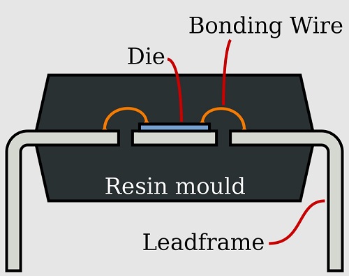
DIP Structure Diagram
DIP packaging follows the JEDEC standard, with a pin spacing of 0.1 inches (2.54 mm). Depending on the number of pins, the distance between the two rows of pins is usually 0.3 inches (7.62 mm) or 0.6 inches (15.24 mm), with less common distances including 0.4 inches (10.16 mm) and 0.9 inches (22.86 mm), and some packages have a special pin spacing of 0.07 inches (1.778 mm), with row spacings of 0.3 inches, 0.6 inches, or 0.75 inches.
The package size directly relates to the device's power capacity and heat dissipation efficiency. Small DIP packages have lower power, while larger packages can handle higher power. Choosing a DIP package requires considering the usage environment and power needs.
DIP packaging always has an even number of pins, with a row spacing of 0.3 inches ranging from 8 to 24 pins, occasionally 4 or 28 pins. 0.6-inch row spacing packaging commonly has 24, 28 pins, and also 32, 40, 36, 48, or 52 pins. CPUs like the Motorola 68000 and Zilog Z180 have up to 64 pins, the maximum for DIP packaging.
6. Orientation and Pin Numbering
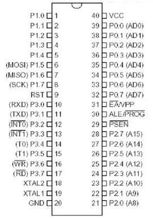
DIP Pinout
When identifying components, if the notch is facing upwards, the top left pin is pin 1, with other pins numbered in a counterclockwise direction. Sometimes, pin 1 is also marked with a dot. The pin layout of DIP packaging closely relates to the device's function and application, and while it may vary for different types of devices, the general pin arrangement is similar.
For example, for a DIP14 IC, when the identification slot is facing upwards, the pins on the left side are numbered from 1 to 7 from top to bottom, and the pins on the right side are numbered from 8 to 14 from bottom to top.
7. Advantages and Disadvantages of DIP
Advantages:
1. Easy to solder: Through-hole mounting technology makes DIP packaging relatively easy for manual or automated soldering.
2. Accessibility: DIP packaging pins are easily accessible, allowing for easy testing, troubleshooting, and insertion.
3. Reliability: DIP packaging provides a secure mechanical connection due to through-hole mounting, making it resistant to mechanical stress and vibration.
2. Accessibility: DIP packaging pins are easily accessible, allowing for easy testing, troubleshooting, and insertion.
3. Reliability: DIP packaging provides a secure mechanical connection due to through-hole mounting, making it resistant to mechanical stress and vibration.
Disadvantages:
1.Large footprint: DIP packaging, due to the same pin distance and pins arranged on both sides, is easy to manufacture but occupies a larger area, which is not conducive to compressing the chip's internal layout.
2. Prone to crosstalk: Due to manufacturing process limitations and the structure of the casing, it does not provide good EMC protection, posing a risk of crosstalk in high-frequency circuits.
3. Higher power consumption: In most systems, the problem with DIP packaging is its relatively large power consumption. It cannot utilize space efficiently, and space limitations can lead to electronic device malfunctions.
8. Characteristics of DIP
DIP packaging is suitable for through-hole soldering on printed circuit boards (PCBs), making it easy to handle. Its chip-to-package volume ratio is larger, resulting in a larger overall size. Early CPUs, such as the 4004, 8008, 8086, and 8088, used this packaging form, allowing insertion into motherboard slots or soldering onto the motherboard.
SDIP (Shrink DIP) is a variant of DIP, with a pin density six times that of DIP. DIP also refers to Dip Switch, with the following electrical characteristics:
- 1. Electrical life: Each switch is tested by moving back and forth 2000 times under a 24V DC voltage and 25mA current;
- 2. Non-frequent switching current rating: 100 mA, 50 VDC voltage resistance;
- 3. DC switch rated voltage and current: 25mA, withstand DC24V;
- 4. Contact resistance: Maximum 50 mΩ: (a) initial value; (b) after testing, we found the maximum value to be 100 mΩ;
- 5. Insulation resistance: Minimum insulation resistance is 100mOhm, 500V DC;
- 6. Dielectric strength: 500VAC/1min;
- 7. Polar Capacitance: 5 pF (maximum);
- 8. Layout: Single-pin radio: DS (S), DP (L).
Additionally, regarding digital aspects of film,
DIP (Digital Image Processor) refers to the secondary practical image
DIP (Digital Image Processor) refers to the secondary practical image
9. Applications of DIP
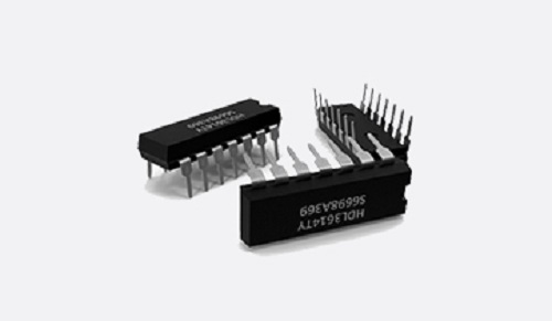
DIP
Integrated circuits often use DIP packaging, as well as DIP switches, LEDs, seven-segment displays, bar graph displays, and relays. Connectors in computers and electronic devices commonly adopt the DIP packaging form.
In 1964, Quick Semiconductor's Bryant Buck Rogers invented the first 14-pin DIP packaging component, which is very similar to the current DIP packaging, with a rectangular shape. Compared to early round components, the rectangular design improves component density on the board. DIP packaging components are suitable for automated assembly, allowing dozens to hundreds of ICs to be soldered onto the board and detected by automated testing equipment, reducing manual operations. Although DIP components are larger than their internal integrated circuits, by the end of the 20th century, surface mount technology (SMT) began to reduce system size and weight. Nevertheless, DIP components are still useful in circuit prototype design, especially when combined with breadboards for easy insertion and replacement.
10. Main Differences Between DIP and SMT
DIP and SMT represent two core electronic component packaging technologies, differing in packaging form, size, soldering process, and performance as follows:
1.Packaging form: DIP uses a traditional packaging method, with component pins arranged for direct insertion into the circuit board through holes and soldering; SMT technology attaches components directly to the circuit board surface and solders them in place.
2. Size and weight: SMT-packaged components are smaller and lighter than DIP, helping to reduce circuit board space and increase board density.
3. Soldering process: DIP packaging involves simple soldering tools for manual or automated soldering; in contrast, SMT requires applying solder paste or conductive adhesive to components, followed by soldering with specialized equipment, making the operation more complex.
4. Performance advantages: SMT components, with shorter pins and lower internal resistance and capacitance, reduce noise and distortion in signal transmission, thus enhancing system performance.
Although DIP still has widespread applications in certain traditional circuit areas, SMT technology has become the mainstream in the electronics manufacturing industry, especially in advanced applications like smart homes, drones, medical equipment, and automotive electronics.
Frequently Asked Questions
What is meant by a dual in-line package?
In microelectronics, a dual in-line package (DIP or DIL) is an electronic component package with a rectangular housing and two parallel rows of electrical connecting pins. The package may be through-hole mounted to a printed circuit board (PCB) or inserted in a socket.
What are the advantages of the dual inline package?
It has many advantages, including being low-cost, easy to assemble, and reliable. DIP stands for the “Dual In-line” design. This refers to the fact that the IC is placed side by side on a Printed Circuit Board (PCB).
What is the difference between a single inline package and a dual inline package?
SIPs are generally plastic packages with a pin count of up to 48 and a pin pitch of 2.54 mm. Dual in-line packages: DIPs come in either plastic or ceramic versions and have two rows of interconnects along two opposite sides of the package.
What is the difference between DIP and DIL?
There is no difference at all. sometimes the P refers to Plastic, so a ceramic part is DIL but not DIP, but these are so rare nowadays that the two terms are equivalent in practice.
About us
ALLELCO LIMITED
Read more
Quick inquiry
Please send an inquiry, we will respond immediately.
→ Previous
The NE555 is a monolithic integrated circuit timer capable of producing various types of timing signals. It is extensively used in electronic clocks, power management, calculators, LED displays, and other electronic devices across various fields. This article aims to provide detailed information abo...
The 78M05 is a linear voltage regulator chip primarily used for stabilizing and filtering DC power supplies. It features built-in circuit protection functions to ensure the safe and stable operation of devices. In this article, we will delve into the 78M05 by exploring its pinout and functions, exte...
→ Next

NE555 introduction, internal structure, operating mode, applications
on March 29th

Comprehensive Understanding of the 78M05 Chip
on March 22th
Popular Posts
-
What is GND in the circuit?
on January 1th 3267
-

RJ-45 Connector Guide: RJ-45 Connector Color Codes, Wiring Schemes, R-J45 Applications, RJ-45 Datasheets
on January 1th 2814
-
Understanding Power Supply Voltages in Electronics VCC, VDD, VEE, VSS, and GND
on November 20th 2631
-

Fiber Connector Types: SC Vs LC And LC Vs MTP
on January 1th 2265
-

Comparison Between DB9 and RS232
on January 1th 1881
-

What Is An LR44 Battery?
Electricity, that ubiquitous force, quietly permeates every aspect of our daily lives, from trivial gadgets to life-threatening medical equipment, it plays a silent role. However, truly grasping this energy, especially how to store and efficiently output it, is no easy task. It is against this background that this article will focus on a type of coin cell battery that may seem insignificant on the...on January 1th 1846
-
Understanding the Fundamentals:Inductance Resistance, andCapacitance
In the intricate dance of electrical engineering, a trio of fundamental elements takes center stage: inductance, resistance, and capacitance. Each bears unique traits that dictate the dynamic rhythms of electronic circuits. Here, we embark on a journey to decipher the complexities of these components, to uncover their distinct roles and practical uses within the vast electrical orchestra. Inductan...on January 1th 1804
-

What Is RF and Why Do We Use It?
Radio Frequency (RF) technology is a key part of modern wireless communication, enabling data transmission over long distances without physical connections. This article delves into the basics of RF, explaining how electromagnetic radiation (EMR) makes RF communication possible. We will explore the principles of EMR, the creation and control of RF signals, and their wide-ranging uses. The article ...on January 1th 1799
-
CR2430 Battery Comprehensive Guide: Specifications, Applications and Comparison to CR2032 Batteries
What is CR2430 battery ?Benefits of CR2430 BatteriesNormCR2430 Battery ApplicationsCR2430 EquivalentCR2430 VS CR2032Battery CR2430 SizeWhat to look for when buying the CR2430 and equivalentsData Sheet PDFFrequently Asked Questions Batteries are the heart of small electronic devices. Among the many types available, coin cells play a crucial role, commonly found in calculators, remote controls, and ...on January 1th 1794
-
Comprehensive guide to hFE in transistors
Transistors are crucial components in modern electronic devices, enabling signal amplification and control. This article delves into the knowledge surrounding hFE, including how to select a transistor's hFE value, how to find hFE, and the gain of different types of transistors. Through our exploration of hFE, we gain a deeper understanding of how transistors work and their role in electronic circu...on November 20th 1782


