Understanding the CD4066B Bilateral Switch
The CD4066B quad bilateral switch is a powerful component, designed to seamlessly handle both analog and digital signals. With its advanced engineering, this device ensures stable, low on-state resistance across a broad input range, making it ideal for applications where signal integrity is a must. Compared to its predecessor, the CD4016B, the CD4066B offers improved signal fidelity and reduced losses, proving valuable for tasks like audio and video processing where clarity and precision are paramount. This versatile switch is an excellent choice for you looking to enhance circuit efficiency, optimize signal paths, and achieve robust performance across diverse conditions.Catalog
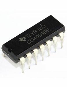
CD4066B Overview
The CD4066B stands out as a remarkable component within the domain of electronic switches, specifically appreciated for its design as a quad bilateral switch. Its ability to proficiently handle both analog and digital signals endows it with a noteworthy versatility, making it suitable for a diverse array of applications such as signal transmission and multiplexing.
When placed alongside the CD4016B, the superiority of the CD4066B becomes evident, primarily due to its lower on-state resistance that remains stable across a variety of signal inputs. This feature is ultimate as it plays a major role in maintaining signal integrity over prolonged periods, while simultaneously minimizing potential distortions that could detract from overall system efficacy.
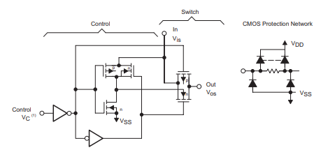
At the core of the CD4066B's functionality are four independent switches, each uniquely controlled by individual signals. This design empowers dynamic and flexible signal routing, thereby enhancing operational efficiency. It also allows for the simultaneous management of multiple signal paths, effectively eliminating any chance of interference. Notably, the incorporation of n-channel devices in each switch fosters a strong connection, either to the input or to VSS (ground). This setup is mostly effective in stabilizing the switch's threshold voltage, which helps maintain consistent resistance during its operations.
Features
|
Feature |
Description |
|
15-V Digital or ±7.5-V Peak-to-Peak Switching |
Operates with a wide switching voltage range. |
|
125-Ω Typical On-State Resistance for 15-V Operation |
Low on-state resistance for efficient switching at 15-V. |
|
Switch On-State Resistance Matched to Within 5 Ω Over
15-V Signal-Input Range |
Ensures consistent performance across the signal range. |
|
On-State Resistance Flat Over Full Peak-to-Peak Signal
Range |
Maintains uniform resistance regardless of signal
variations. |
|
High On or Off Output-Voltage Ratio |
80 dB typical at fis = 10 kHz, RL = 1 kΩ, for superior
signal isolation. |
|
High Degree of Linearity |
<0.5% distortion typical at fis = 1 kHz, Vis = 5-Vp-p,
VDD – VSS ≥ 10-V, RL = 10 kΩ. |
|
Extremely Low Off-State Switch Leakage |
Very low offset current and high effective off-state
resistance: 10 pA typical at VDD – VSS = 10-V, TA = 25°C. |
|
Extremely High Control Input Impedance |
10¹² Ω typical; isolates control circuit from the signal
circuit. |
|
Low Crosstalk Between Switches |
–50 dB typical at fis = 8 MHz, RL = 1 kΩ, for minimal
interference. |
|
Matched Control-Input to Signal-Output Capacitance |
Reduces output signal transients for better stability. |
|
Frequency Response, Switch On |
40 MHz typical, enabling high-speed switching. |
|
100% Tested for Quiescent Current at 20-V |
Ensures quality and reliability for low power
consumption. |
|
5-V, 10-V, and 15-V Parametric Ratings |
Compatible with multiple voltage levels for versatile
applications. |
Pin Configuration
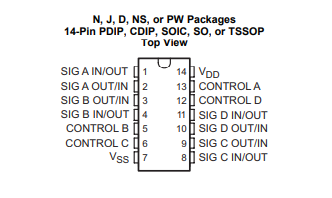
|
NO. |
NAME |
I/O |
DESCRIPTION |
|
1 |
SIG A IN/OUT |
I/O |
Input/Output for Switch A |
|
2 |
SIG A OUT/IN |
I/O |
Output/Input for Switch A |
|
3 |
SIG B OUT/IN |
I/O |
Output/Input for Switch B |
|
4 |
SIG B IN/OUT |
I/O |
Input/Output for Switch B |
|
5 |
CONTROL B |
I |
Control pin for Switch B |
|
6 |
CONTROL C |
I |
Control pin for Switch C |
|
7 |
VSS |
— |
Low Voltage Power Pin |
|
8 |
SIG C IN/OUT |
I/O |
Input/Output for Switch C |
|
9 |
SIG C OUT/IN |
I/O |
Output/Input for Switch C |
|
10 |
SIG D OUT/IN |
I/O |
Output/Input for Switch D |
|
11 |
SIG D IN/OUT |
I/O |
Input/Output for Switch D |
|
12 |
CONTROL D |
I |
Control Pin for D |
|
13 |
CONTROL A |
I |
Control Pin for A |
|
14 |
VDD |
— |
Power Pin |
Technical Specifications
Here is the technical specifications table for Texas Instruments CD4066BE.
|
Type |
Parameter |
|
Lifecycle Status |
ACTIVE (Last Updated: 1 day ago) |
|
Factory Lead Time |
6 Weeks |
|
Contact Plating |
Gold |
|
Mount |
Through Hole |
|
Mounting Type |
Through Hole |
|
Package / Case |
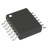
14-DIP (0.300, 7.62mm) |
|
Number of Pins |
14 |
|
Weight |
927.99329mg |
|
Turn Off Delay Time |
30 ns |
|
Operating Temperature |
-55°C ~ 125°C |
|
Packaging |
Tube |
|
Series |
4000B |
|
JESD-609 Code |
e3 |
|
Part Status |
Active |
|
Moisture Sensitivity Level (MSL) |
1 (Unlimited) |
|
Number of Terminations |
14 |
|
ECCN Code |
EAR99 |
|
Type |
Bilateral, FET Switches |
|
Resistance |
240Ohm |
|
Terminal Finish |
Matte Tin (Sn) |
|
Voltage - Supply |
3V ~ 18V |
|
Number of Functions |
4 |
|
Supply Voltage |
5V |
|
Frequency |
40MHz |
|
Base Part Number |
CD4066 |
|
Pin Count |
14 |
|
Number of Outputs |
2 |
|
Circuit |
1 x 1:1 |
|
Polarity |
Non-Inverting |
|
Power Supplies |
5/15V |
|
Number of Channels |
4 |
|
Max Supply Current |
5μA |
|
Throw Configuration |
SPST |
|
Quiescent Current |
20nA |
|
Turn On Delay Time |
30 ns |
|
Number of Inputs |
3 |
|
Supply Type |
Dual, Single |
|
Bandwidth |
40MHz |
|
Neg Supply Voltage-Nom (Vsup) |
-5V |
|
Max Dual Supply Voltage |
9V |
|
Min Dual Supply Voltage |
1.5V |
|
Dual Supply Voltage |
7.5V |
|
Input Capacitance |
8pF |
|
Voltage Supply Source |
Dual Supply |
|
On-state Resistance Match-Nom |
15Ohm |
|
Switching |
BREAK-BEFORE-MAKE |
|
Switch-on Time-Max |
70ns |
|
Switch-off Time-Max |
70ns |
|
Drain to Source Resistance |
470Ohm |
|
Normal Position |
NO |
|
Ambient Temperature Range High |
125°C |
|
Height |
5.08mm |
|
Length |
19.3mm |
|
Width |
6.35mm |
|
Thickness |
3.9mm |
|
REACH SVHC |
No SVHC |
|
Radiation Hardening |
No |
|
RoHS Status |
ROHS3 Compliant |
|
Lead Free |
Lead Free |
CD4066B Use Cases
The CD4066B showcases its versatility across a diverse array of applications, mostly in the areas of analog switching and multiplexing. Its unique ability to gate and modulate signals bolsters its significance within various electronic frameworks. A prime illustration of the CD4066B’s utility emerges in situations that demand agile control over analog signals. For example, in audio processing systems, this component adeptly manages audio signal routing, selectively activating or deactivating channels to elevate functionality and enrich your experience.
Analog Signal Switching
In the domain of analog signal switching, the CD4066B fulfills various roles, including that of a variable resistor and a conventional switch. This versatility allows for meticulous adjustments to both signal amplitude and phase, an attribute that proves advantageous in scenarios where exacting control over signal qualities is active. In audio mixing consoles, engineers routinely manipulate multiple signals. The CD4066B empowers them to define specific pathways for distinct signals, ultimately achieving a more polished audio output.
Digital Signal Switching
The functionality of the CD4066B in facilitating digital signal switching and multiplexing greatly extends its range of applications. Digital circuits, play a major part in managing data flow effectively, ensuring that digital signals traverse without distortion. When integrated into microcontroller-based projects, where various sensors vie for access to a single communication line, the CD4066B proficiently coordinates multiple sensor inputs, toggling between them as circumstances dictate. Its adaptability to interface effortlessly with various communication protocols enhances its effectiveness. For instance, in systems utilizing I2C or SPI protocols, the CD4066B can skillfully switch between different peripheral devices. This capability conserves board space and amplifies overall design efficiency.
Automation and Control Systems
The significance of the CD4066B in automation within various control systems warrants attention. Its use enables digital governance over serious parameters such as frequency, impedance, phase, and gain. In smart home environments, the device can regulate lighting modulation, adjusting light intensities based on factors like time of day or occupancy. This responsiveness not only promotes energy savings but also enhances overall comfort. Moreover, the ability to tailor these controls according to specific environmental cues showcases the essence of your design in modern systems. The evolution from manual operations to automated solutions marks a defining trend in contemporary electronic design, inspiring you to innovate thoughtfully and incorporate components like the CD4066B to achieve both functional and aesthetic aspirations.
Datasheet PDF
CD4066BE Datasheets:
About us
ALLELCO LIMITED
Read more
Quick inquiry
Please send an inquiry, we will respond immediately.
Frequently Asked Questions [FAQ]
1. How does a bilateral switch work?
A bilateral switch enables current to flow in both directions, offering unmatched flexibility in a wide range of electrical applications. Unlike traditional unidirectional switches, any terminal of a bilateral switch can function as an input, thanks to advancements in semiconductor technologies, mostly field-effect transistors (FETs), which ensure rapid switching for modern electronic devices. Its adaptable design supports various scenarios, from simple audio devices to complex digital signal routing, making it invaluable in both analog and digital contexts. In analog systems, bilateral switches enable smooth signal processing with minimal resistance, preserving input signal quality and reducing distortion—a serious factor in high-fidelity audio applications. In addition, these switches simplify circuit connections during prototyping, saving time and minimizing errors, while in final designs, they streamline layouts to create compact, efficient, and reliable circuit boards, embodying the pursuit of optimized engineering solutions.
All About the M95512-R 512-Kbit EEPROM: Pinout, Datasheet, and Substitutes
on November 15th
What You Need to Know About the TSAL6100 Infrared LED?
on November 15th
Popular Posts
-
What is GND in the circuit?
on January 1th 3280
-

RJ-45 Connector Guide: RJ-45 Connector Color Codes, Wiring Schemes, R-J45 Applications, RJ-45 Datasheets
on January 1th 2817
-
Understanding Power Supply Voltages in Electronics VCC, VDD, VEE, VSS, and GND
on November 20th 2651
-

Fiber Connector Types: SC Vs LC And LC Vs MTP
on January 1th 2268
-

Comparison Between DB9 and RS232
on January 1th 1886
-

What Is An LR44 Battery?
Electricity, that ubiquitous force, quietly permeates every aspect of our daily lives, from trivial gadgets to life-threatening medical equipment, it plays a silent role. However, truly grasping this energy, especially how to store and efficiently output it, is no easy task. It is against this background that this article will focus on a type of coin cell battery that may seem insignificant on the...on January 1th 1847
-
Understanding the Fundamentals:Inductance Resistance, andCapacitance
In the intricate dance of electrical engineering, a trio of fundamental elements takes center stage: inductance, resistance, and capacitance. Each bears unique traits that dictate the dynamic rhythms of electronic circuits. Here, we embark on a journey to decipher the complexities of these components, to uncover their distinct roles and practical uses within the vast electrical orchestra. Inductan...on January 1th 1811
-
What Is RF and Why Do We Use It?
Radio Frequency (RF) technology is a key part of modern wireless communication, enabling data transmission over long distances without physical connections. This article delves into the basics of RF, explaining how electromagnetic radiation (EMR) makes RF communication possible. We will explore the principles of EMR, the creation and control of RF signals, and their wide-ranging uses. The article ...on January 1th 1808
-

CR2430 Battery Comprehensive Guide: Specifications, Applications and Comparison to CR2032 Batteries
What is CR2430 battery ?Benefits of CR2430 BatteriesNormCR2430 Battery ApplicationsCR2430 EquivalentCR2430 VS CR2032Battery CR2430 SizeWhat to look for when buying the CR2430 and equivalentsData Sheet PDFFrequently Asked Questions Batteries are the heart of small electronic devices. Among the many types available, coin cells play a crucial role, commonly found in calculators, remote controls, and ...on January 1th 1804
-
Comprehensive guide to hFE in transistors
Transistors are crucial components in modern electronic devices, enabling signal amplification and control. This article delves into the knowledge surrounding hFE, including how to select a transistor's hFE value, how to find hFE, and the gain of different types of transistors. Through our exploration of hFE, we gain a deeper understanding of how transistors work and their role in electronic circu...on November 20th 1786


