SS8550 Transistor: Specifications, Alternatives, and Pinout
The SS8550 transistor is a small but powerful piece of electronic hardware. It’s a PNP silicon transistor that can handle high currents up to 1.5 amps, while working well in low-voltage setups. Because it’s so versatile and reliable, the SS8550 shows up in all kinds of electronic projects, from power management systems to audio amplifiers. Its ability to adapt to different needs makes it a popular choice and it plays a role in many modern electronic designs.Catalog

What is the SS8550 Transistor?
The SS8550 is a PNP transistor often chosen for its adaptability across a range of electronic applications. Known for managing low voltage with a capacity to support high current, it has a collector current maximum of 1.5 A. Such qualities promote its utilization in circuits requiring efficient low-voltage amplification or adept switching operations. The capability of this transistor to handle substantial current at low voltage is highly valuable in power management circuits, audio amplifiers, and signal processing units. Its reliable current management makes it suitable for both analog and digital circuits.
SS8550 Equivalent
• SS9012
• SS9015
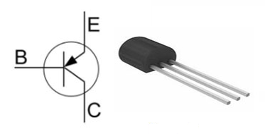
SS8550 Pin Configuration
|
Pin Number |
Pin Name |
Description |
|
1 |
Emitter |
The emitter pin releases charge carriers. In circuit
applications, its correct orientation is good for improving current flow and
ensuring the transistor's stability. |
|
2 |
Base |
Acts as the control gate by regulating the flow of
charges from the emitter to the collector. Modulating the base current is key
for adjusting amplification levels for achieving desired performance
in circuit configurations. |
|
3 |
Collector |
The endpoint for collecting charge carriers. Proper
connection and alignment are needed to maximize efficiency and minimize
energy loss, as misalignments can impact the performance of the
circuit. |
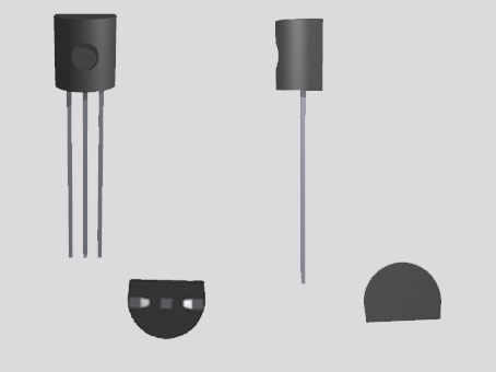
SS8550 Symbol, Footprint, CAD Model


SS8550 Transistor Features
The SS8550 transistor is renowned for its substantial operational proficiency, most notably as a 2W output amplifier, perfectly suited for portable radios using Class B push-pull configurations. It pairs effortlessly with the SS8050 counterpart, forming a powerful electronic duo that amplifies the performance of compact devices. A thorough examination of its properties highlights a collector-base voltage of 40V and a power dissipation capacity of 1W under thermal conditions.
Its design accommodates a broad temperature range from -55°C to +150°C, allowing it to function reliably across various environments. The SS8550 adheres to RoHS standards, reflecting a dedication to environmentally friendly manufacturing, in line with global sustainability movements. There is a notable interplay between adherence to such standards and preferences, indicating that compliance not only safeguards the environment but also boosts confidence.
SS8550 Technical Specifications
Technical specifications, attributes, and parameters of ON Semiconductor's SS8550, along with parts similar to the SS8550DBU.
|
Type |
Parameter |
|
Lifecycle Status |
ACTIVE (Last Updated: 2 days ago) |
|
Mount |
Through Hole |
|
Package / Case |
TO-226-3, TO-92-3 (TO-226AA) |
|
Weight |
179mg |
|
Collector-Emitter Breakdown Voltage |
25V |
|
hFE Min |
85 |
|
Packaging |
Bulk |
|
JESD-609 Code |
e3 |
|
Part Status |
Active |
|
Number of Terminations |
3 |
|
Terminal Finish |
Tin (Sn) |
|
Max Power Dissipation |
1W |
|
Current Rating |
-1.5A |
|
Base Part Number |
SS8550 |
|
Factory Lead Time |
7 Weeks |
|
Mounting Type |
Through Hole |
|
Number of Pins |
3 |
|
Transistor Element Material |
SILICON |
|
Number of Elements |
1 |
|
Operating Temperature |
150°C TJ |
|
Published |
2017 |
|
Pbfree Code |
yes |
|
Moisture Sensitivity Level (MSL) |
1 (Unlimited) |
|
ECCN Code |
EAR99 |
|
Voltage - Rated DC |
-25V |
|
Terminal Position |
BOTTOM |
|
Frequency |
200MHz |
|
Element Configuration |
Single |
|
Power Dissipation |
1W |
|
Gain Bandwidth Product |
200MHz |
|
Transistor Application |
AMPLIFIER |
|
Polarity/Channel Type |
PNP |
|
Collector Emitter Voltage (VCEO) |
25V |
|
DC Current Gain (hFE) (Min) @ Ic, Vce |
160 @ 100mA 1V |
|
Vce Saturation (Max) @ Ib, Ic |
500mV @ 80mA, 800mA |
|
Collector Base Voltage (VCBO) |
-40V |
|
Transition Frequency |
200MHz |
|
Emitter Base Voltage (VEBO) |
-6V |
|
Current - Collector Cutoff (Max) |
100nA ICBO |
|
Max Collector Current |
1.5A |
|
Radiation Hardening |
No |
|
Lead Free |
Lead Free |
|
REACH SVHC |
No SVHC |
|
RoHS Status |
ROHS3 Compliant |
Alternatives of SS8550
|
Part Number |
Description |
Manufacturer |
|
SS8550DBU |
1500mA, 25V, PNP, Si, SMALL SIGNAL TRANSISTOR, TO-92 |
Rochester Electronics LLC |
|
SS8550DBU |
Through Hole, Collector Emitter Breakdown Voltage 25 V,
Max Collector Current 1.5 A, Transition Frequency 200 MHz, Collector Emitter
Saturation Voltage -280 mV, hFE Min 85, Max Power Dissipation 1 W |
ON Semiconductor |
|
KSB564AOBU |
Through Hole, Collector Emitter Breakdown Voltage 25 V,
Max Collector Current 1.5 A, Transition Frequency 200 MHz, Collector Emitter
Saturation Voltage -280 mV, hFE Min 85, Max Power Dissipation 1 W |
ON Semiconductor |
|
SS8550CBU |
Through Hole, Collector Emitter Breakdown Voltage 25 V,
Max Collector Current 1.5 A, Transition Frequency 200 MHz, Collector Emitter
Saturation Voltage -280 mV, hFE Min 85, Max Power Dissipation 1 W |
ON Semiconductor |
|
SS8550BBU |
Through Hole, Collector Emitter Breakdown Voltage 25 V,
Max Collector Current 1 A, Collector Emitter Saturation Voltage -500 mV, hFE
Min 70, Max Power Dissipation 800 W |
ON Semiconductor |
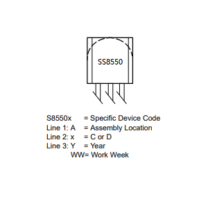
Marking Diagram of SS8550
Applications of SS8550
The SS8550 transistor finds extensive use in both switching and RF (Radio Frequency) applications, showcasing its extraordinary adaptability. This component is valued for its substantial current gain and impressive frequency capabilities, characteristics that enhance its effectiveness in signal amplification and electrical current management across a wide range of electronic systems. Its integration into various devices highlights the importance of choosing components with precise specifications for achieving excellent performance. Particularly in communication devices, its proficiency in handling high frequencies plays a role in sustaining signal integrity and clarity, integral aspects in today's swiftly evolving technological world.
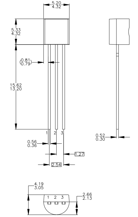
SS8550 Packaging
SS8550 Manufacturer Information
ON Semiconductor stands out by crafting advanced silicon solutions that enhance the operational efficiency of electronic devices across various applications. Focusing on sectors such as automotive, communications, and LED lighting, they blend sophisticated technologies with sustainable practices. As society greatly craves energy-efficient innovations, ON Semiconductor's contributions increasingly address these desires. ON Semiconductor prioritizes the creation of eco-friendly products, drawing on their expansive industry knowledge. Their resolve extends to minimizing environmental impact through cutting-edge manufacturing techniques, reflecting a synergy with worldwide sustainability objectives. This effort shapes a more sustainable pathway in electronics production.
Datasheet PDF
SS8550DBU Datasheets:
Copper Lead Frame 12/Oct/2007.pdf
SS8550CBU Datasheets:
Copper Lead Frame 12/Oct/2007.pdf
About us
ALLELCO LIMITED
Read more
Quick inquiry
Please send an inquiry, we will respond immediately.
Frequently Asked Questions [FAQ]
1. What characterizes a common triode?
A triode, such as the SS8550, plays a role in signal amplification, capturing the essence of converting faint whispers of electrical signals into more discernible ones. In electronic circuits, it elevates weak signals to levels that can be effectively utilized. Functioning with a subtle touch at its base, the triode facilitates a more substantial current flow between the collector and emitter, enabling precise signal modulation. An insightful choice of triode, tailored to the desired circuit, depends on a keen understanding of parameters like gain, frequency response, and thermal stability. When designing circuits, harnessing these characteristics can unlock the potential across various applications, ranging from the resonant melodies of audio equipment to the expansive reach of communication devices.
2. What is the peak collector current capability?
The SS8550 can handle a peak collector current of 1.5 A, marking its threshold before excessive heat or electrical stress threaten its well-being. Vigilant thermal management is needed, as exceeding this current may lead to thermal runaway, a perilous surge in temperature with destructive potential for the transistor. Implementing measures such as heat sinks or selecting components with a naturally higher current tolerance can serve as safeguards against such risks. Maintaining the transistor within safe operational limits is an art that enhances the longevity and reliability of the device, reflecting a deep respect for its delicate balance.
LM393N Comparator IC Explained
on November 8th
A Complete Guide to the OV7670 Camera Module
on November 8th
Popular Posts
-
What is GND in the circuit?
on January 1th 3095
-

RJ-45 Connector Guide: RJ-45 Connector Color Codes, Wiring Schemes, R-J45 Applications, RJ-45 Datasheets
on January 1th 2661
-
Understanding Power Supply Voltages in Electronics VCC, VDD, VEE, VSS, and GND
on November 14th 2188
-

Fiber Connector Types: SC Vs LC And LC Vs MTP
on January 1th 2176
-

Comparison Between DB9 and RS232
on January 1th 1799
-

What Is An LR44 Battery?
Electricity, that ubiquitous force, quietly permeates every aspect of our daily lives, from trivial gadgets to life-threatening medical equipment, it plays a silent role. However, truly grasping this energy, especially how to store and efficiently output it, is no easy task. It is against this background that this article will focus on a type of coin cell battery that may seem insignificant on the...on January 1th 1773
-
Understanding the Fundamentals:Inductance Resistance, andCapacitance
In the intricate dance of electrical engineering, a trio of fundamental elements takes center stage: inductance, resistance, and capacitance. Each bears unique traits that dictate the dynamic rhythms of electronic circuits. Here, we embark on a journey to decipher the complexities of these components, to uncover their distinct roles and practical uses within the vast electrical orchestra. Inductan...on January 1th 1726
-
CR2430 Battery Comprehensive Guide: Specifications, Applications and Comparison to CR2032 Batteries
What is CR2430 battery ?Benefits of CR2430 BatteriesNormCR2430 Battery ApplicationsCR2430 EquivalentCR2430 VS CR2032Battery CR2430 SizeWhat to look for when buying the CR2430 and equivalentsData Sheet PDFFrequently Asked Questions Batteries are the heart of small electronic devices. Among the many types available, coin cells play a crucial role, commonly found in calculators, remote controls, and ...on January 1th 1668
-
What Is RF and Why Do We Use It?
Radio Frequency (RF) technology is a key part of modern wireless communication, enabling data transmission over long distances without physical connections. This article delves into the basics of RF, explaining how electromagnetic radiation (EMR) makes RF communication possible. We will explore the principles of EMR, the creation and control of RF signals, and their wide-ranging uses. The article ...on January 1th 1666
-
Comprehensive guide to hFE in transistors
Transistors are crucial components in modern electronic devices, enabling signal amplification and control. This article delves into the knowledge surrounding hFE, including how to select a transistor's hFE value, how to find hFE, and the gain of different types of transistors. Through our exploration of hFE, we gain a deeper understanding of how transistors work and their role in electronic circu...on November 14th 1617
