CD4011 Nand Gate IC: Datasheet, Pinout, and Features
This article provides a comprehensive examination of the CD4011 integrated circuit, a key member of the CMOS family, renowned for its four integrated NAND gates. It delves into the pinout specifics, variations by manufacturers such as Texas Instruments, and available alternatives to the CD4011. The discussion extends to the practical implications and the broader impact of this chip on digital circuit design, emphasizing its role in enhancing system reliability and performance across various applications.Catalog

What is the CD4011?
The CD4011 is an intriguing integration of four 2-input NAND gates, forming an important part of the flexible CD40xx CMOS IC series. These NAND gates hold a role in digital electronics by delivering a LOW output exclusively when all their inputs are in a HIGH state, otherwise, they sustain a HIGH output. This distinct characteristic makes the NAND gate a foundational element in logic circuit design, providing adaptability through universal gate logic that can be engineered to perform a variety of operations, such as AND, OR, and NOT functions. A noteworthy aspect of the CD4011 is its swift transition time. In practical deployment, this facilitates accelerated signal processing, ensuring prompt and effective shifts in logic states. Such an attribute becomes highly beneficial in environments that demand speed, like computing and systems requiring responsive control.
The transformation of a NAND gate into a NOT gate by merging its inputs illustrates the CD4011's adaptability. This flexibility in logic design allows for a reduction in the number of components within an IC. In scenarios where compact and efficient circuit architectures are called for, the capacity to execute various logic functions with minimal hardware turns into a significant advantage. Aligning the output voltage of the CD4011 with its operational voltage accentuates its compatibility and facilitates smoother interfacing with other components working at identical voltage levels. This feature reduces the risk of mismatches and eases the integration process into larger systems.
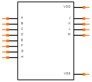
CD4011 Pin Configuration
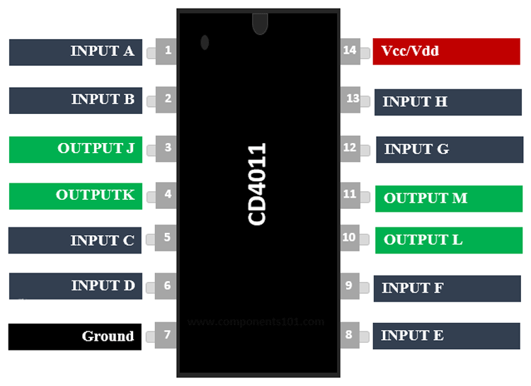
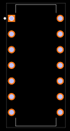
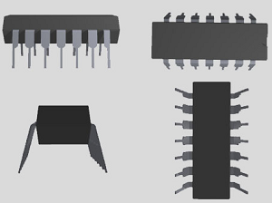
CD4011 Symbol, Footprint, and CAD Model
Features of the CD4011
Dual Input NAND Gate Arrangement
The CD4011 features four independent NAND gates, each designed with dual inputs and enclosed within a compact 14-pin package. This arrangement supports efficient logic processes across a wide spectrum of digital applications, adding a layer of adaptability with voltage operations at 5V, complemented by options for 10V and 15V. This adaptability, meeting varied operational scenarios with consistent performance, often charms those crafting intricate circuitry designs.
Electrical Characteristics
Central to the CD4011's allure is its output current of 1.5mA, catering to a multitude of interfacing needs. Its typical propagation delay is 60 ns, a compelling trait for those engaged in high-speed digital processing projects.
Operating Range Resilience
The CD4011 operates reliably within a temperature span of -55°C to +125°C, ensuring functionality under extreme conditions. This resilience makes it a favored component for aerospace and industrial purposes, where exposure to severe temperatures is routine. The ability to endure such conditions shows its trustworthiness, akin to elements in systems where lapses are inconceivable.
Package Options
The CD4011 comes in various 14-pin package formats, offering the flexibility needed to accommodate different design constraints. This adaptability aids those aiming to maximize space efficiency and reduce costs. Strategically selecting a package type that aligns with the mechanical requirements of a project demonstrates a careful approach to component integration.
Buffered Inputs/Outputs and Symmetrical Performances
Incorporating buffered inputs and outputs bolsters the signal integrity and steadiness of data. Symmetrical outputs further enhance balanced functioning, an aspect highly valued in precision-dependent circuits. The even transition of signals between stages is a testament to the precision achieved through years of design evolution and practical insights.
Noise Margin and Quiescent Current
The robust noise margins of the CD4011 render it less vulnerable to electrical noise, markedly enhancing circuit dependability. The necessity of strong noise margins for maintaining performance in disruptive environments. Testing for quiescent current at 20V minimizes parasitic power usage, aligning smoothly with energy-conscious design practices.
CD4011 Technical Specifications
Technical specifications, attributes, parameters, and components similar to the CD4011BE from Texas Instruments.
|
Type |
Parameter |
|
Lifecycle Status |
ACTIVE (Last Updated: 4 days ago) |
|
Contact Plating |
Gold |
|
Mounting Type |
Through Hole |
|
Number of Pins |
14 |
|
Logic Level-High |
3.5V ~ 11V |
|
Operating Temperature |
-55°C~125°C |
|
Series |
4000B |
|
Part Status |
Active |
|
Number of Terminations |
14 |
|
ECCN Code |
EAR99 |
|
Terminal Position |
DUAL |
|
Supply Voltage |
5V |
|
Pin Count |
14 |
|
Max Output Current |
6.8mA |
|
Factory Lead Time |
8 Weeks |
|
Mount |
Through Hole |
|
Package / Case |
14-DIP (0.300, 7.62mm) |
|
Weight |
927.99329mg |
|
Logic Level-Low |
1.5V ~ 4V |
|
Packaging |
Tube |
|
JESD-609 Code |
e4 |
|
Moisture Sensitivity Level (MSL) |
1 (Unlimited) |
|
Termination |
Through Hole |
|
Voltage - Supply |
3V~18V |
|
Number of Functions |
4 |
|
Base Part Number |
CD4011 |
|
Number of Outputs |
1 |
|
Supply Voltage-Min (Vsup) |
3V |
|
Number of Channels |
4 |
|
Power Dissipation |
100mW |
|
Propagation Delay |
90 ns |
|
Turn On Delay Time |
90 ns |
|
Number of Inputs |
2 |
|
Max (Io) |
0.0068 A |
|
Input Capacitance |
5pF |
|
Current - Quiescent (Max) |
1µA |
|
Height |
5.08mm |
|
Width |
6.35mm |
|
REACH SVHC |
No SVHC |
|
Lead Free |
Lead Free |
|
Load Capacitance |
50pF |
|
Output Current |
6.8mA |
|
Quiescent Current |
5µA |
|
Logic Function |
NAND |
|
Logic Type |
NAND Gate |
|
Max Propagation Delay @ V, Max CL |
90ns @ 15V, 50pF |
|
Power Supply Current-Max (ICC) |
0.03mA |
|
Schmitt Trigger Input |
No |
|
Length |
19.3mm |
|
Thickness |
3.9mm |
|
RoHS Status |
ROHS3 Compliant |
CD4011 Utilization
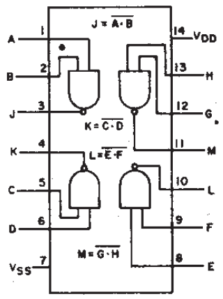
The CD4011 is not just any quad NAND gate integrated circuit; it forms the core of countless electronic applications. Connect its Vcc and ground pins to a standard 5V power supply for optimal functionality. The CD4011 chip has 12 pins and includes four NAND gates. To use the CD4011, you need to connect it to power (Vcc) and ground. It usually works with a +5V power supply but can also handle +7V. The output voltage matches the power you supply to the chip. For a NAND gate, the output is high (on) only when both inputs are low (off). In any other case, the output stays low (off).
Applications and Uses of CD4011
AV Receivers
The CD4011 is integral in elevating AV receivers, enhancing the intricacies of signal processing. This optimization allows for a spectrum of high-quality audio and video outputs, meeting the sophisticated tastes drawn to refined home entertainment experiences.
Blu-ray Players
In the core of Blu-ray players, the CD4011 is good for decoding and processing data with efficiency. Its integration boosts playback quality and system dependability, making every viewing moment a delight to the senses.
Home Theaters
Robustness and seamless integration form the backbone of home theater systems. The CD4011 ensures intricate management of both audio and video, offering an immersive cinematic experience in their personal sanctuaries.
Portable Audio Docks
Employing the CD4011 in portable audio docks enhances signal amplification and sound clarity, crafting a rich, immersive audio during travel. It ensures uniformity across diverse audio formats and sources, appealing to auditory purists.
MP3 Players/Recorders
In MP3 players and recorders, the CD4011 orchestrates digital signals and data encoding efficiently. By optimizing power consumption, it extends device operations and refines performance, a primary pursuit for innovators aiming to maximize battery longevity.
Personal Digital Assistants (PDAs)
Within PDAs, the CD4011's adaptability shines through its capability to manage varied input/output functions. It optimizes computational processes and power usage, facilitating multitasking, a core aspect of contemporary PDAs focused on productivity enhancement.
Decoders and Multiplexers
The CD4011 plays a role in decoders and multiplexers by guaranteeing precise signal routing and handling. This precision aligns with the needs of industries such as telecommunications and data transmission, where reliability and accuracy are non-negotiable.
Logic Gates and Audio Players
In the logic gates, the CD4011 is important for digital circuit creation. In audio players, it refines audio signal processing, ensuring sound reproduction that satisfies high-fidelity expectations.
Digital Locks and Safety Thermostats
Integrating the CD4011 within digital locks and safety thermostats elevates the reliability and reactivity of these systems. It bolsters secure access and precise temperature regulation for safeguarding spaces in both residential and commercial settings.
Alternatives of the CD4011
|
Part Number |
Manufacturer |
Description |
|
M38510/05001BCX |
Texas Instruments |
4000/14000/40000 SERIES, QUAD 2-INPUT NAND GATE, CDIP14,
CERAMIC, DIP-14 |
|
5962R9662104VCX |
Harris Semiconductor |
NAND Gate, 4000/14000/40000 Series, 4-Func, 2-Input,
CMOS, CDIP14 |
|
M38510H05051SCA |
Defense Logistics Agency |
NAND Gate, 4000/14000/40000 Series, 4-Func, 2-Input,
CMOS, CDIP14, CERAMIC, DIP-14 |
|
MM54C00N |
Texas Instruments |
TTL/H/L SERIES, QUAD 2-INPUT NAND GATE, PDIP14, DIP-14 |
|
CD4011AE |
Texas Instruments |
4000/14000/40000 SERIES, QUAD 2-INPUT NAND GATE, PDIP14,
PLASTIC, DIP-14 |
|
MC14011UBCP |
ON Semiconductor |
4000/14000/40000 SERIES, QUAD 2-INPUT NAND GATE, PDIP14 |
|
HEF4011BP |
NXP Semiconductors |
4000/14000/40000 SERIES, QUAD 2-INPUT NAND GATE, PDIP14,
0.300 INCH, PLASTIC, SC501-14, M-001, SOT27-1, DIP-14 |
|
MC14011BCP |
Freescale Semiconductor |
IC, LOGIC GATE, QUAD 2-INPUT NAND, CMOS, DIP,14PIN,
PLASTIC |
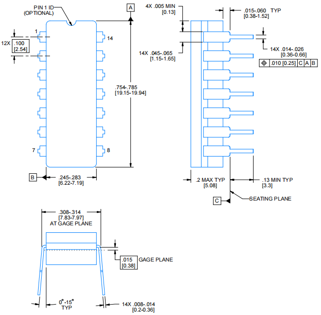
Package for CD4011
CD4011 Manufacturer Information
Texas Instruments (TI), with its headquarters nestled in the vibrant heart of Dallas, Texas, is a prominent player within the semiconductor industry. The allure of TI's specialization in analog chips and embedded processing, coupled with its remarkable portfolio boasting over 45,000 patents, illustrates TI's unwavering dedication to pioneering advancements and technological progress. This vast compilation of patents is a testament to TI's enduring impact and leadership in sculpting the future of the semiconductor world. In the rapidly shifting semiconductor landscape, TI's blueprint for growth embraces expansion and flexibility. Future growth is intertwined with a fusion of groundbreaking innovation and responsiveness to the flux of market dynamics. Texas Instruments embodies a paragon of strategic vision and innovation in the semiconductor sphere. Through its defined specialization, expansive patent collection, and practical implementations, TI not only fortifies but enhances its role worldwide.
Datasheet PDF
CD4011BE Datasheets:
Cylindrical Battery Holders.pdf
MC14011UBCP Datasheets:
Multiple Devices 20/Aug/2008.pdf
About us
ALLELCO LIMITED
Read more
Quick inquiry
Please send an inquiry, we will respond immediately.
Frequently Asked Questions [FAQ]
1. What is CD4011?
The CD4011 is a CMOS device that includes four 2-input NAND gates. It provides a high output only when both inputs receive a low signal; otherwise, the output remains low. This device is appreciated for its ability to function within a wide voltage range from 3V to 18V, which can be appealing for varying applications. These applications may range from basic logic operations to intricate power-sensitive environments. The capacity to handle such voltage variability is beneficial for optimizing circuit performance and achieving greater efficiency.
2. What is the difference between CD4011 and 74HC00P?
Both the CD4011 and the 74HC00P house four 2-input NAND gates but differ in pin layout and voltage operation. The CD4011 supports a broad voltage range of 3V to 18V, while the 74HC00P operates within a tighter 2V to 6V range. These attributes influence their usage under distinct power conditions. In devices relying on low-voltage batteries, the 74HC00P may be advantageous, whereas the CD4011 could be more suitable for systems with higher voltage demands.
3. What is the difference between CD4093 and CD4011?
While both the CD4093 and CD4011 include four 2-input NAND gates and share similar pin configurations, a prominent distinction is the CD4093’s incorporation of a Schmitt trigger. This addition enhances the CD4093’s effectiveness in scenarios with fluctuating or slow input signals, lending it better noise immunity and smoother signal transitions. In circuit designs where input stability poses a challenge, employing a component like the CD4093 can bolster signal reliability and precision. The choice between these components often hinges on the specific signal conditioning needs inherent in the circuit's design.
OPA2134 Audio Operational Amplifier: Pinout, Equivalents, and Features
on November 6th
Differences Between RG6 and RG11 Coaxial Cables
on November 5th
Popular Posts
-
What is GND in the circuit?
on January 1th 2881
-

RJ-45 Connector Guide: RJ-45 Connector Color Codes, Wiring Schemes, R-J45 Applications, RJ-45 Datasheets
on January 1th 2458
-

Fiber Connector Types: SC Vs LC And LC Vs MTP
on January 1th 2055
-
Understanding Power Supply Voltages in Electronics VCC, VDD, VEE, VSS, and GND
on November 7th 1826
-

Comparison Between DB9 and RS232
on January 1th 1746
-

What Is An LR44 Battery?
Electricity, that ubiquitous force, quietly permeates every aspect of our daily lives, from trivial gadgets to life-threatening medical equipment, it plays a silent role. However, truly grasping this energy, especially how to store and efficiently output it, is no easy task. It is against this background that this article will focus on a type of coin cell battery that may seem insignificant on the...on January 1th 1698
-
Understanding the Fundamentals:Inductance Resistance, andCapacitance
In the intricate dance of electrical engineering, a trio of fundamental elements takes center stage: inductance, resistance, and capacitance. Each bears unique traits that dictate the dynamic rhythms of electronic circuits. Here, we embark on a journey to decipher the complexities of these components, to uncover their distinct roles and practical uses within the vast electrical orchestra. Inductan...on January 1th 1641
-

CR2430 Battery Comprehensive Guide: Specifications, Applications and Comparison to CR2032 Batteries
What is CR2430 battery ?Benefits of CR2430 BatteriesNormCR2430 Battery ApplicationsCR2430 EquivalentCR2430 VS CR2032Battery CR2430 SizeWhat to look for when buying the CR2430 and equivalentsData Sheet PDFFrequently Asked Questions Batteries are the heart of small electronic devices. Among the many types available, coin cells play a crucial role, commonly found in calculators, remote controls, and ...on January 1th 1512
-
What Is RF and Why Do We Use It?
Radio Frequency (RF) technology is a key part of modern wireless communication, enabling data transmission over long distances without physical connections. This article delves into the basics of RF, explaining how electromagnetic radiation (EMR) makes RF communication possible. We will explore the principles of EMR, the creation and control of RF signals, and their wide-ranging uses. The article ...on January 1th 1499
-

CR2450 vs CR2032: Can The Battery Be Used Instead?
Lithium manganese batteries do have some similarities with other lithium batteries. High energy density and long service life are the characteristics they have in common. This kind of battery has won the trust and favor of many consumers because of its unique safety. Expensive tech gadgets? Small appliances in our homes? Look around and you'll see them everywhere. Among these many lithium-manganes...on January 1th 1482
