A Complete Guide to the CD4046BE and Its Applications
This article provides a detailed look into the CD4046BE, a widely used Phase-Locked Loop (PLL) integrated circuit, covering its operation, key features, and practical applications. It also explains how PLL systems work, focusing on their ability to synchronize signals for various uses in electronics, communications, and signal processing. We'll dive into how the CD4046BE works in systems like radar, frequency synthesis, and clock recovery, along with its technical parameters, pin configuration, and real-world implementation. Finally, a FAQ section will address common questions about the CD4046BE.Catalog
Understanding a Phase-Locked Loop
A Phase-Locked Loop (PLL) is an electronic system that controls and synchronizes frequencies. It works by aligning the frequency or phase of a voltage-controlled oscillator (VCO) with an input signal, ensuring accuracy and stability. A phase comparator plays a key role in this process.
The key components of a PLL are the phase detector, loop filter, and voltage-controlled oscillator. The phase detector compares the input signal's phase to the VCO’s output and reduces any differences. The loop filter processes the output from the phase detector and creates a stable control voltage for the VCO, which helps reduce noise and keeps the system steady. The VCO then adjusts its output to match the input signal, keeping the frequencies synchronized.
PLLs are used in many industries. In digital communications, they synchronize data transmission for faster, more reliable networks. In consumer electronics like TVs and radios, they maintain stable signals for clear audio and video. In industrial automation, they ensure precise control of machinery, improving efficiency and accuracy in manufacturing.
New uses for PLLs are also emerging. They can improve the efficiency of power systems in renewable energy and enhance synchronization in sensor networks for the Internet of Things (IoT). Understanding how Phase-Locked Loops work highlights their role in modern technology.
CD4046BE In-Depth Analysis
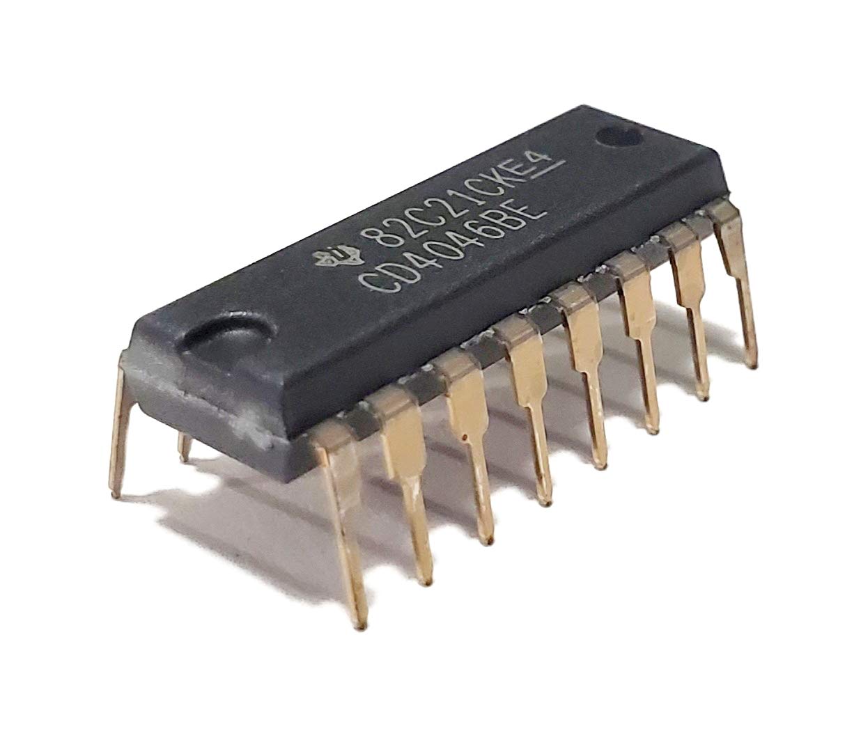
The CD4046BE is a versatile CMOS Phase-Locked Loop (PLL) integrated circuit with an internal oscillator, error detector, and dual phase comparators, all housed in a 16-pin Dual In-line Package (DIP). It is commonly used in applications related to frequency and timing, making it useful for generating clock signals for microcontrollers, demodulating FM signals, and recovering clock signals in digital communication systems. This IC proves to be highly effective in digital receiver setups where precise timing is required.
The CD4046BE’s ability to generate accurate clock signals is due to its internal oscillator, which is fine-tuned to meet the timing needs of various microcontroller applications. This accuracy is especially important in devices like audio and video systems, where smooth operation depends on synchronized timing.
In FM signal demodulation, the CD4046BE uses its phase comparators and error detector to convert signals accurately, a key feature in radio communications where clear signal transmission is necessary. The IC also performs well in digital communication systems by recovering clock signals from data streams. This stabilization reduces transmission errors and improves the overall reliability of data in communication networks.
Equivalent Models
• CD4046BF
• MC14046BCPD
• NTE4046BE
Symbol, Footprint, and Pin Configuration of CD4046BE
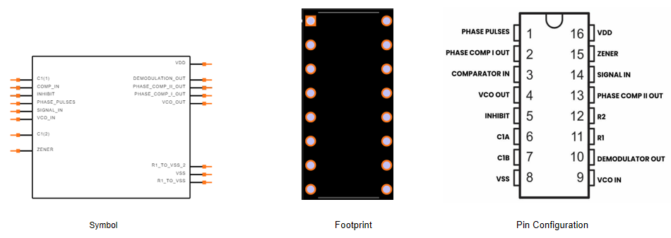
The CD4046BE has 16 pins, each with a specific role in operating the phase-locked loop (PLL) circuit. These pins help manage various functions like oscillator control and signal processing, making the IC adaptable for different applications.
CD4046BE Configuration and Pins
• PHASE PULSES
The PHASE PULSES pin shows the lock status of the PLL, helping users monitor the system’s performance. By checking the phase between the input and the oscillator signal, users can determine if the PLL is locked. In communication systems, engineers frequently use this pin to troubleshoot synchronization issues, making it a helpful diagnostic tool.
• VCO OUT
The VCO OUT pin provides the signal from the Voltage-Controlled Oscillator (VCO), which creates a frequency based on the input control voltage. This pin is used in frequency modulation and demodulation tasks. The VCO’s precision directly impacts the performance of systems that depend on specific frequencies. This pin plays a key role in controlling frequencies in such systems.
• INHIBIT
The INHIBIT pin controls whether the VCO is active or not. By activating this pin, the VCO can be turned off, which is useful for saving power or during testing. Engineers often rely on this pin when debugging or performing maintenance to isolate PLL issues, making it a practical tool in real-world applications.
• PHASE COMP I OUT and PHASE COMP II OUT
These pins output signals from the two phase comparators in the CD4046BE. Phase Comparator I ensures zero phase error between input signals, ideal for applications requiring precise phase matching. Phase Comparator II offers stable output over a wider frequency range, giving more flexibility. Engineers select which output to use based on their specific project needs, such as choosing Phase Comparator I when accuracy in timing is required.
Key Features of CD4046BE
Lock Indicator Pin
The lock indicator pin helps maintain the quality of the signal by confirming when the PLL has locked onto the correct frequency. This prevents the signal from drifting and ensures stable performance. This feature is particularly useful in systems where signal synchronization is needed, like communication networks, where timing must stay precise.
Wide Voltage Range
The CD4046BE can work within a wide voltage range, from 3V to 18V, which allows it to perform consistently even when there are changes in voltage. This flexibility makes it a good choice for devices powered by batteries and industrial applications. In these environments, the ability to handle different voltage levels helps ensure the equipment runs smoothly, even when the power supply is unstable.
Low Power Consumption
With a low power usage of just 600μW at 10kHz, the CD4046BE is a great option for applications that need to run continuously over long periods. Its low power consumption extends the life of battery-powered devices and reduces the heat generated during operation. This makes it ideal for mobile technology and wearable devices, where both long battery life and durability are needed.
High Input Impedance
The CD4046BE has a high input impedance of up to 100MΩ, which helps reduce signal loss and improves overall performance. A high input impedance puts less strain on the signal source, which is especially useful in high-frequency applications. This feature is valuable in devices requiring high signal accuracy, such as medical instruments, where maintaining signal quality is essential.
Tunable Oscillator
The CD4046BE includes a tunable oscillator that allows precise control of the output frequency by adjusting the external voltage. This feature makes the IC adaptable to a wide range of uses, such as audio equipment and digital clock generation. The ability to fine-tune the frequency provides greater control and improves the overall reliability of the system.
These features make the CD4046BE a highly reliable component for various applications. Its balance of power efficiency, stability, and flexibility makes it a strong choice for building advanced electronic systems that require both high performance and long-term durability.
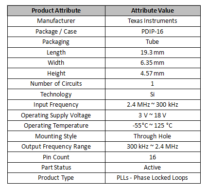
CD4046BE Technical Parameters
CD4046BE Operation
The CD4046BE is a phase-locked loop (PLL) integrated circuit that synchronizes an input signal with a reference signal. It starts with the phase detector, which compares the two signals and generates an error signal based on their phase difference. This error signal goes through a low-pass filter to remove noise, leaving a stable DC voltage that controls the voltage-controlled oscillator (VCO). The VCO adjusts its frequency to match the reference signal.
Fine-tuning the low-pass filter helps improve the system's response and reduces jitter, ensuring more stable frequency tracking, especially in telecommunications. The VCO output feeds back into the phase detector, creating a loop that continuously corrects any phase or frequency shifts.
The CD4046BE is often used in frequency synthesis to generate different frequencies from a single reference clock. This is crucial in radio transmitters and receivers, where accurate frequency control is needed. By carefully configuring the VCO in the PLL circuit, high-frequency accuracy and stability are achieved, which is essential in wireless communications for reducing interference and optimizing bandwidth.
Applications of CD4046BE
Doppler Frequency Measurement
The CD4046BE is widely used in radar systems to detect movement by measuring Doppler frequency shifts. This function helps track target speed and changes in frequency. It has improved the accuracy of radar-based systems, such as air traffic control and weather forecasting, where precise detection of movement is needed.
Frequency Synthesis
The CD4046BE is effective in generating accurate clock signals by comparing reference signals with its internal oscillations. This ensures stable frequency generation, which is important for systems that need precise timekeeping and synchronization. In telecommunications, for example, proper frequency synthesis helps maintain the reliability of signal transmission and keeps communication networks running smoothly.
Clock Recovery
In digital communications, the CD4046BE is useful for recovering clock signals from incoming data, which allows for correct demodulation. This helps maintain data accuracy and ensures smooth communication. In modem technology, the ability to recover lost signals has been a key factor in improving data transmission.
Oscillator Control
The CD4046BE provides precise control of frequency and phase in oscillators, making it adaptable to various applications. It’s especially valuable in systems that need to adjust to different operational conditions. For instance, in signal processing, fine-tuning the oscillator settings can improve performance, showing how versatile the chip is in different technical setups.
Practical Implementation of the CD4046BE
When implementing the CD4046BE, start by selecting the appropriate modulation method and carrier signal for your application. Techniques like Binary Phase Shift Keying (BPSK) or Quadrature Amplitude Modulation (QAM) are common options, depending on your system needs. This selection process often requires careful evaluation of factors such as bandwidth efficiency and signal strength, as the choice of modulation method directly impacts the system’s performance and reliability.
Next, ensure proper integration of the CD4046BE with both modulator and demodulator components. Signal levels need to be compatible to avoid any loss in signal quality. For example, impedance matching is a common practice to preserve signal integrity. At this stage, it's also important to configure settings such as the Voltage-Controlled Oscillator (VCO) frequency range, filter type, and frequency division ratio, as these parameters directly influence system stability.
Once the modulator is set up, the digital signal is converted into an analog signal and sent over a carrier, with the CD4046BE processing it efficiently. Proper adjustment of modulation parameters can minimize distortion and ensure clear transmission. In data communication systems, precision during this digital-to-analog conversion is key to achieving higher data rates and reducing transmission errors.
To recover the original digital signal, the CD4046BE demodulates the analog output back into its digital form. Ensuring accurate signal recovery is critical for maintaining data quality. Fine-tuning the phase-locked loop (PLL) components helps achieve precise signal restoration, a technique often used in radio frequency systems to maintain high signal fidelity.
Finally, thorough testing and debugging are necessary to confirm the system’s performance. Tools like spectrum analyzers and oscilloscopes are often used to assess the CD4046BE’s operation. Iterative testing and adjustments, such as modifying filter bandwidth or tweaking the VCO control voltage, can significantly improve overall system reliability.
Frequently Asked Questions [FAQ]
1. What is CD4046?
The CD4046 is a versatile Micropower Phase-Locked Loop (PLL) integrated circuit designed to synchronize input and output signal phases. This makes it useful in many applications that need accurate phase locking and synchronization.
2. How does CD4046 work?
The CD4046 combines a phase comparator, a low-pass filter (LPF), and a voltage-controlled oscillator (VCO) in a feedback loop. The phase comparator adjusts the VCO’s frequency to match the input signal, keeping the system synchronized. This process is commonly used in fields like communications and signal processing to ensure signal consistency.
3. What is the CD4046BE power supply range?
The CD4046BE can operate with a power supply ranging from 3 volts to 18 volts. This wide range makes it suitable for both low-power and high-power systems, giving it flexibility in various applications.
4. What is PLL?
A Phase-Locked Loop (PLL) is an electronic system that synchronizes the phase of an output signal with an input signal. It usually includes a frequency oscillator and a phase detector in a feedback loop. PLLs are commonly used in tasks like frequency synthesis, clock generation, and signal demodulation, ensuring signals stay synchronized over different distances and conditions in communication systems.
5. What is the loop filter's role in CD4046BE?
The loop filter in the CD4046BE helps stabilize the control voltage sent to the VCO. It smooths out voltage fluctuations, ensuring a steady phase relationship between input and output signals. This stability is crucial for accurately modulating and demodulating signals in communication systems, helping maintain data integrity during transmission and reception.
About us
ALLELCO LIMITED
Read more
Quick inquiry
Please send an inquiry, we will respond immediately.
TL3845P PWM Controller: Pinout, Key Features, and Layout Tips
on September 27th
Everything You Need to Know About the LM2575 Voltage Regulator
on September 27th
Popular Posts
-
What is GND in the circuit?
on January 1th 3103
-

RJ-45 Connector Guide: RJ-45 Connector Color Codes, Wiring Schemes, R-J45 Applications, RJ-45 Datasheets
on January 1th 2671
-
Understanding Power Supply Voltages in Electronics VCC, VDD, VEE, VSS, and GND
on November 15th 2209
-

Fiber Connector Types: SC Vs LC And LC Vs MTP
on January 1th 2182
-

Comparison Between DB9 and RS232
on January 1th 1802
-

What Is An LR44 Battery?
Electricity, that ubiquitous force, quietly permeates every aspect of our daily lives, from trivial gadgets to life-threatening medical equipment, it plays a silent role. However, truly grasping this energy, especially how to store and efficiently output it, is no easy task. It is against this background that this article will focus on a type of coin cell battery that may seem insignificant on the...on January 1th 1774
-
Understanding the Fundamentals:Inductance Resistance, andCapacitance
In the intricate dance of electrical engineering, a trio of fundamental elements takes center stage: inductance, resistance, and capacitance. Each bears unique traits that dictate the dynamic rhythms of electronic circuits. Here, we embark on a journey to decipher the complexities of these components, to uncover their distinct roles and practical uses within the vast electrical orchestra. Inductan...on January 1th 1728
-

CR2430 Battery Comprehensive Guide: Specifications, Applications and Comparison to CR2032 Batteries
What is CR2430 battery ?Benefits of CR2430 BatteriesNormCR2430 Battery ApplicationsCR2430 EquivalentCR2430 VS CR2032Battery CR2430 SizeWhat to look for when buying the CR2430 and equivalentsData Sheet PDFFrequently Asked Questions Batteries are the heart of small electronic devices. Among the many types available, coin cells play a crucial role, commonly found in calculators, remote controls, and ...on January 1th 1673
-
What Is RF and Why Do We Use It?
Radio Frequency (RF) technology is a key part of modern wireless communication, enabling data transmission over long distances without physical connections. This article delves into the basics of RF, explaining how electromagnetic radiation (EMR) makes RF communication possible. We will explore the principles of EMR, the creation and control of RF signals, and their wide-ranging uses. The article ...on January 1th 1670
-
Comprehensive guide to hFE in transistors
Transistors are crucial components in modern electronic devices, enabling signal amplification and control. This article delves into the knowledge surrounding hFE, including how to select a transistor's hFE value, how to find hFE, and the gain of different types of transistors. Through our exploration of hFE, we gain a deeper understanding of how transistors work and their role in electronic circu...on November 15th 1629
HOT Part Number
-

PIC16LF1707-I/P
Microchip Technology
IC MCU 8BIT 3.5KB FLASH 20DIP
LQP03HQ2N0B02D
Murata Electronics
FIXED IND 2NH 600MA 120MOHM SMD
SN74ALVCH16245DGGR
Texas Instruments
IC TXRX NON-INVERT 3.6V 48TSSOP
QS8F2TCR
Rohm Semiconductor
MOSFET/TRANS P-CH/PNP TSMT8
9012-05-11
Coto Technology
RELAY REED SPST 500MA 5V
1N2979A
Microchip Technology
DIODE ZENER 15V 10W DO213AA
0603ZD105KAT2A
KYOCERA AVX
CAP CER 1UF 10V X5R 0603
SMAJ75A-E3/61
Vishay General Semiconductor - Diodes Division
TVS DIODE 75VWM 121VC DO214AC
PT7M7825RTAEX
Diodes Incorporated
IC SUPERVISOR 1 CHANNEL SOT23-5
MK20DX256VLQ10R
NXP USA Inc.
IC MCU 32BIT 256KB FLASH 144LQFP
CC0603CRNPO0BN3R3
YAGEO
CAP CER 3.3PF 100V C0G/NPO 0603
GRM188R61A224KA01D
Murata Electronics
CAP CER 0.22UF 10V X5R 0603
GRT21BC81E475KA02L
Murata Electronics
CAP CER 4.7UF 25V X6S 0805
NVMFS5C430NLWFT1G
onsemi
MOSFET N-CH 40V 200A 5DFN
BZV55-C12,115
Nexperia USA Inc.
DIODE ZENER 12V 500MW LLDS
725964-2
TE Connectivity AMP Connectors
CONN QC TAB 0.250 SOLDER
GRM1887U2A3R7CZ01D
Murata Electronics
CAP CER 3.7PF 100V U2J 0603
SN74LV4066ADRG4
Texas Instruments
IC SWITCH QUAD 1X1 14SOIC -

MCP1727T-3302E/MF
Microchip Technology
IC REG LINEAR 3.3V 1.5A 8DFN
ATB2012-75011M-T000
TDK Corporation
RF BALUN 400-1800MHZ 2DB 2012
ZMV830BTA
Diodes Incorporated
DIODE VARACTOR 25V HYPER SOD-323
DG441DJ
Analog Devices Inc./Maxim Integrated
IC SWITCH SPST-NCX4 85OHM 16DIP
UPD6P8MC-5A4-A
Renesas Electronics America Inc
4-BIT, OTPROM, 4MHZ
51021-0400
Molex
1.25 WTB REC HSG 4CKT 4CKT 1.25M
0402YC103KA72A
KYOCERA AVX
CAP CER 10000PF 16V X7R 0402
DM74ALS373WMX
Fairchild Semiconductor
BUS DRIVER
GRM2197U2A6R3DD01D
Murata Electronics
CAP CER 6.3PF 100V U2J 0805
EM357-RTR
Silicon Labs
IC RF TXRX+MCU 802.15.4 48VFQFN
GCM1885C2A750JA16D
Murata Electronics
CAP CER 75PF 100V C0G/NP0 0603
GRM1886R1H7R8DZ01D
Murata Electronics
CAP CER 7.8PF 50V R2H 0603
LM2575S-12
Texas Instruments
IC REG BUCK 12V 1A TO263-5
ST72F324LJ4T6
STMicroelectronics
IC MCU 8BIT 16KB FLASH 44LQFP
749069-9
TE Connectivity AMP Connectors
CONN D-TYPE RCPT 100P VERT SLDR
M30260F8AGP#U5A
Renesas Electronics America Inc
IC MCU 16BIT 64KB FLASH 48LFQFP
TMDS261BPAG
Texas Instruments
IC VIDEO HDMI/DVI SWITCH 64TQFP
74VCX162373MTDX
onsemi
IC LATCH TRANSP 16BIT LV 48TSSOP -

SS10PH10HM3/86A
Vishay General Semiconductor - Diodes Division
DIODE SCHOTTKY 100V 10A TO277A
10M02DCU324I7G
Intel
IC FPGA 160 I/O 324UBGA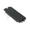
STK6712BMK4-E
onsemi
UNIPOLAR FIXED-CURRENT CHOPPER-T
MAX5190BEEG+T
Analog Devices Inc./Maxim Integrated
IC DAC 8BIT V-OUT 24QSOP
C0402CH1C680K020BC
TDK Corporation
CAP CER 68PF 16V CH 01005
SI2300DS-T1-GE3
Vishay Siliconix
MOSFET N-CH 30V 3.6A SOT23-3
SLF6025T-150MR88-PF
TDK Corporation
FIXED IND 15UH 1.1A 102 MOHM SMD
71V3577S80BQI
IDT, Integrated Device Technology Inc
IC SRAM 4.5MBIT PAR 165CABGA
MCP79402-I/MS
Microchip Technology
IC RTC CLK/CALENDAR I2C 8MSOP
CY8C20066A-24LTXI
Infineon Technologies
IC CAPSENSE PSOC 32K 48QFN
JMK107BJ225MV-T
Taiyo Yuden
CAP CER 2.2UF 6.3V X5R 0603
LX1682CDM
Microsemi Corporation
IC REG CTRLR BUCK 8SOIC
AS4C32M16D2A-25BCN
Alliance Memory, Inc.
IC DRAM 512MBIT PARALLEL 84FBGA
PS11014
Powerex Inc.
MOD IPM 3PHASE IGBT 600V 15A
LP2957ISX
Texas Instruments
IC REG LIN 5V 250MA DDPAK/TO263
RT1206BRE0721KL
YAGEO
RES SMD 21K OHM 0.1% 1/4W 1206
VI-24Y-CW
Vicor Corporation
DC DC CONVERTER 3.3V 20W
NVD5407NT4G
onsemi
MOSFET N-CH 40V 7.6A/38A DPAK