View All

Please refer to the English Version as our Official Version.Return

Europe
France(Français) Germany(Deutsch) Italy(Italia) Russian(русский) Poland(polski) Netherlands(Nederland) Spain(español) Turkey(Türk dili) Israel(עִבְרִית) Denmark(Dansk) Switzerland(Deutsch) United Kingdom(English)
Asia/Pacific
Japan(日本語) Korea(한국의) Thailand(ภาษาไทย) Malaysia(Melayu) Singapore(Melayu) Philippines(Pilipino)
Africa, India and Middle East
India(हिंदी)
North America
United States(English) Canada(English) Mexico(español)
HomeProductsDiscrete Semiconductor ProductsTransistors - FETs, MOSFETs - SingleFQD18N20V2TM
FQD18N20V2TM Image
Image may be representation.
See specifications for product details.

FQD18N20V2TM - onsemi

Manufacturer Part Number
FQD18N20V2TM
Manufacturer
onsemi
Allelco Part Number
32D-FQD18N20V2TM
ECAD Model
Parts Description
MOSFET N-CH 200V 15A DPAK
Detailed Description
Package
TO-252-3, DPak (2 Leads + Tab), SC-63
Data sheet
FQD18N20V2.pdf
RoHs Status
ROHS3 Compliant
In stock: 81930

Required fields are indicated by an asterisk (*)
Please send RFQ, we will respond immediately.

Quantity

Specifications

FQD18N20V2TM Tech Specifications
onsemi - FQD18N20V2TM technical specifications, attributes, parameters and parts with similar specifications to onsemi - FQD18N20V2TM

Product Attribute Attribute Value  
Manufacturer onsemi  
Vgs(th) (Max) @ Id 5V @ 250µA  
Vgs (Max) ±30V  
Technology MOSFET (Metal Oxide)  
Supplier Device Package TO-252AA  
Series QFET®  
Rds On (Max) @ Id, Vgs 140mOhm @ 7.5A, 10V  
Power Dissipation (Max) 2.5W (Ta), 83W (Tc)  
Package / Case TO-252-3, DPak (2 Leads + Tab), SC-63  
Package Tape & Reel (TR)  
Product Attribute Attribute Value  
Operating Temperature -55°C ~ 150°C (TJ)  
Mounting Type Surface Mount  
Input Capacitance (Ciss) (Max) @ Vds 1080 pF @ 25 V  
Gate Charge (Qg) (Max) @ Vgs 26 nC @ 10 V  
FET Type N-Channel  
FET Feature -  
Drive Voltage (Max Rds On, Min Rds On) 10V  
Drain to Source Voltage (Vdss) 200 V  
Current - Continuous Drain (Id) @ 25°C 15A (Tc)  
Base Product Number FQD18N20  

Parts Introduction

Manufacturer Part Number

FQD18N20V2TM

Manufacturer

onsemi

Introduction

High-voltage, N-channel power MOSFET

Product Features and Performance

Rated for 200 V drain-to-source voltage

Low on-resistance of 140 mΩ typical

Capable of 15 A continuous drain current at 25°C

Product Advantages

Low gate charge for efficient switching

Excellent thermal performance with up to 83 W power dissipation

Wide operating temperature range of -55°C to 150°C

Key Technical Parameters

Drain-to-Source Voltage (Vdss): 200 V

Gate-to-Source Voltage (Vgs): ±30 V

On-Resistance (Rds(on)): 140 mΩ @ 7.5 A, 10 V

Drain Current (Id): 15 A @ 25°C

Input Capacitance (Ciss): 1080 pF @ 25 V

Power Dissipation (Ptot): 2.5 W @ 25°C, 83 W @ 25°C

Quality and Safety Features

RoHS3 compliant

Suitable for surface mount applications

Compatibility

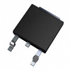
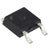
TO-252-3, DPak (2 Leads + Tab), SC-63 package

Application Areas

Switching power supplies

Motor drives

Industrial and consumer electronics

Product Lifecycle

Current product, no plans for discontinuation

Replacements and upgrades available

Key Reasons to Choose This Product

High voltage rating up to 200 V

Low on-resistance for efficient power conversion

Excellent thermal performance for high power applications

Wide operating temperature range for reliable operation

Compact surface mount package for space-constrained designs

Parts with Similar Specifications

The three parts on the right have similar specifications to onsemi FQD18N20V2TM

Product Attribute FQD18N20V2TM FQD19N10TM FQD19N10LTM FQD19N10LTF
Part Number FQD18N20V2TM FQD19N10TM FQD19N10LTM FQD19N10LTF
Manufacturer onsemi Fairchild Semiconductor onsemi Fairchild Semiconductor
Series QFET® QFET® QFET® QFET®
Vgs (Max) ±30V ±25V ±20V ±20V
Operating Temperature -55°C ~ 150°C (TJ) -55°C ~ 150°C (TJ) -55°C ~ 150°C (TJ) -55°C ~ 150°C (TJ)
Technology MOSFET (Metal Oxide) MOSFET (Metal Oxide) MOSFET (Metal Oxide) MOSFET (Metal Oxide)
Package Tape & Reel (TR) Bulk Tape & Reel (TR) Bulk
Gate Charge (Qg) (Max) @ Vgs 26 nC @ 10 V 25 nC @ 10 V 18 nC @ 5 V 18 nC @ 5 V
Power Dissipation (Max) 2.5W (Ta), 83W (Tc) 2.5W (Ta), 50W (Tc) 2.5W (Ta), 50W (Tc) 2.5W (Ta), 50W (Tc)
Drain to Source Voltage (Vdss) 200 V 100 V 100 V 100 V
Base Product Number FQD18N20 - FQD19N10 -
Supplier Device Package TO-252AA TO-252, (D-Pak) TO-252AA TO-252, (D-Pak)
FET Feature - - - -
Vgs(th) (Max) @ Id 5V @ 250µA 4V @ 250µA 2V @ 250µA 2V @ 250µA
Drive Voltage (Max Rds On, Min Rds On) 10V 10V 5V, 10V 5V, 10V
Input Capacitance (Ciss) (Max) @ Vds 1080 pF @ 25 V 780 pF @ 25 V 870 pF @ 25 V 870 pF @ 25 V
Rds On (Max) @ Id, Vgs 140mOhm @ 7.5A, 10V 100mOhm @ 7.8A, 10V 100mOhm @ 7.8A, 10V 100mOhm @ 7.8A, 10V
Current - Continuous Drain (Id) @ 25°C 15A (Tc) 15.6A (Tc) 15.6A (Tc) 15.6A (Tc)
Package / Case TO-252-3, DPak (2 Leads + Tab), SC-63 TO-252-3, DPak (2 Leads + Tab), SC-63 TO-252-3, DPak (2 Leads + Tab), SC-63 TO-252-3, DPak (2 Leads + Tab), SC-63
Mounting Type Surface Mount Surface Mount Surface Mount Surface Mount
FET Type N-Channel N-Channel N-Channel N-Channel

FQD18N20V2TM Datasheet PDF

Download FQD18N20V2TM pdf datasheets and onsemi documentation for FQD18N20V2TM - onsemi.

Datasheets
FQD18N20V2.pdf
Environmental Information
onsemi REACH.pdf onsemi RoHS.pdf
PCN Design/Specification
Logo 17/Aug/2017.pdf Description Chg 01/Apr/2016.pdf
PCN Packaging
Mult Devices 24/Oct/2017.pdf Tape and Box/Reel Barcode Update 07/Aug/2014.pdf
PCN Assembly/Origin
Assembly Change 28/May/2023.pdf

Shipment

Delivery Time

In-stock items can be shipped within 24 hours. Some parts will be arranged for delivery within 1-2 days from the date all items arrive at our warehouse. And Allelco ships order once a day at about 17:00, except Sunday. Once the goods are shipped, the estimated delivery time depends on the shipping methods and Delivery destination. The table below shows are the logistic time for some common countries.

Delivery Cost

  1. Use your express account for shipment if you have one.
  2. Use our account for the shipment. Refer to the table below for the approximate charges.
(Different time frame / countries / package size has different price.)

Delivery Method

  1. Global Common Shipment by DHL / UPS / FedEx / TNT / EMS / SF we support.
  2. Others more shipping ways, please get in touch with your customer manager.

Common Countries Logistic Time Reference
Region Country Logistic Time(Day)
America United States 5
Brazil 7
Europe Germany 5
United Kingdom 4
Italy 5
Oceania Australia 6
New Zealand 5
Asia India 4
Japan 4
Middle East Israel 6
DHL & FedEx Shipment Charges Reference
Shipment charges(KG) Reference DHL(USD$)
0.00kg-1.00kg USD$30.00 - USD$60.00
1.00kg-2.00kg USD$40.00 - USD$80.00
2.00kg-3.00kg USD$50.00 - USD$100.00
Note:
The above table is for reference only. There may have some data bias for the uncontrollable factors.
Contact us if you have any questions.

Payment Support

The payment method can be chosen from the methods shown below: Wire Transfer (T/T, Bank Transfer), Western Union, Credit card, PayPal.

Your Faithful Supply Chain Partner -

Contact us if you have any questions.

  1. Phone
    +00852 9146 4856

Certifications & Memberships

View More
FQD18N20V2TM Image

FQD18N20V2TM

onsemi
32D-FQD18N20V2TM

Want a better price? Add to Cart and Submit RFQ now, we'll contact you immediately.

0 RFQ
Shopping cart (0 Items)
It is empty.
Compare List (0 Items)
It is empty.
Feedback

Your feedback matters! At Allelco, we value the user experience and strive to improve it constantly.
Please share your comments with us via our feedback form, and we'll respond promptly.
Thank you for choosing Allelco.

Subject
E-mail
Comments
Captcha
Drag or click to upload file
Upload File
types: .xls, .xlsx, .doc, .docx, .jpg, .png and .pdf.
Max file size: 10MB