Understanding the Power of the S-R Latch: A Gateway to Modern Electronics
Latches are simple digital devices that store one bit of information and keep that value until it gets new input signals. They are used in digital systems to temporarily hold binary data. Latches can be made using different kinds of basic logic gates like AND, OR, NOT, NAND, and NOR gates. This article explores the design, function, variations, and uses of the S-R latch, emphasizing its best role in modern electronics and its use in practical circuits and digital logic simulations.
Catalog
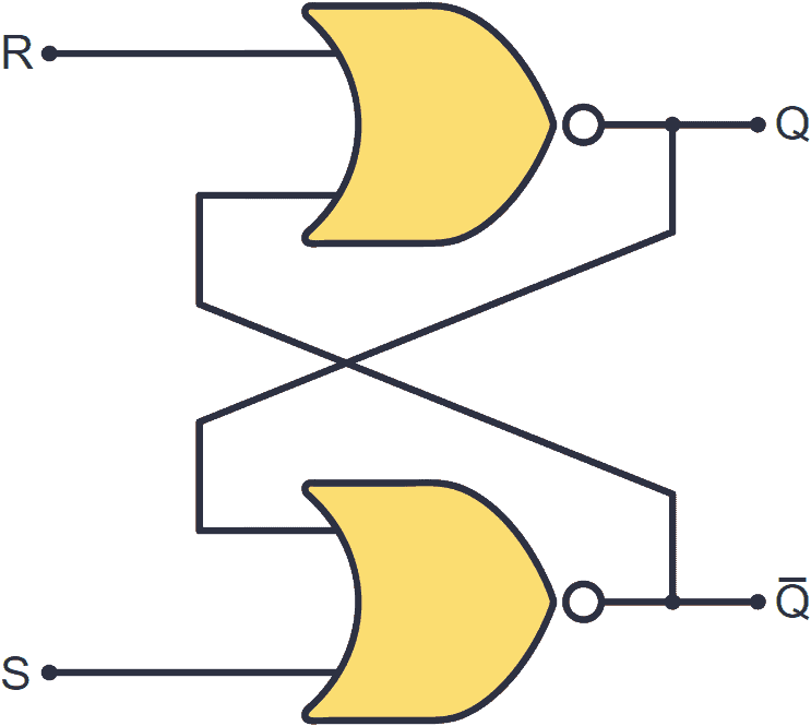
Figure 1: S-R Latch Circuit Diagram
Structure of the S-R Latch
The S-R (Set-Reset) latch, a cornerstone in digital electronics, is a bistable multivibrator. It is capable of maintaining one of two distinct, stable states indefinitely without external input. This functionality renders the SR latch a main component in memory storage and switching operations across different electronic devices.
Structurally, the SR latch consists of two interconnected NOR gates arranged in a feedback loop design. This specific arrangement matters since it offers the prerequisites for bistability. Each NOR gate's output is connected directly to the input of the other, creating a continuous loop of feedback that underpins the latch’s operation.
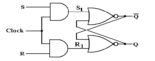
Figure 2: S-R Latch and the Clock Signal (CLK)
Expanding on the basic design, the Gated SR latch introduces an additional, input: the clock signal (CLK). This enhancement incorporates a clock input that brings layer of control, integrating the latch operations into systems that require synchronization. This synchronization obliged as it determines the precise moments when the latch can change states, aptly described by the term "gated." The inclusion of the clock signal ensures that changes to the latch’s output state only occur during the active clock phase, typically at the rising or falling edge of the CLK signal.
The introduction of the CLK input not only preserves the properties of the basic SR latch but also aligns its operation with the temporal dynamics of larger digital systems. This alignment desire for maintaining data integrity and ensuring that the state transitions occur without glitches or unintended changes, particularly in complex circuit configurations where multiple latches may interact. By controlling when the latch responds to the Set and Reset commands, the system can avoid issues such as race conditions and other timing-related errors that might otherwise disrupt system stability and performance.
Operational States of the S-R Latch
Its operation depends on the inputs of two control signals: Set (S) and Reset (R). Here, we explain how these inputs affect the outputs and the states of the SR Latch.
Case 1: Set Condition
When the Set (S) input is high (1) and the Reset (R) input is low (0), the latch enters the Set condition. In this state, the NAND gate connected to the R input will output a low signal because of the high input from S. This low signal causes the second NAND gate to output a high signal, setting Q to high (1) and Q-bar to low (0). This state is stable and will keep Q high until the inputs change, showing the latch's ability to store a high state.
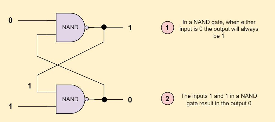
Figure 3: The Set State
Case 2: Reset Condition
When S is low (0) and R is high (1), the latch enters the Reset condition. Here, the high input on R and the low input on S make the NAND gate connected to R output a low signal. This low signal sets Q to low (0) and Q-bar to high (1), effectively resetting the latch. This demonstrates the latch's ability to return to a stable low state in Q when given the right inputs.
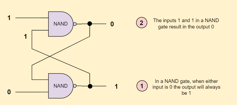
Figure 4: The Reset State
Case 3: Invalid State
If both S and R are low (0), both inputs to the NAND gates are low, causing both outputs Q and Q-bar to go high. This state is called invalid or forbidden because it breaks the basic rule that Q and Q-bar should always be opposites. This scenario highlights the limitation of the SR latch, emphasizing the importance of avoiding such unstable states through proper input management.
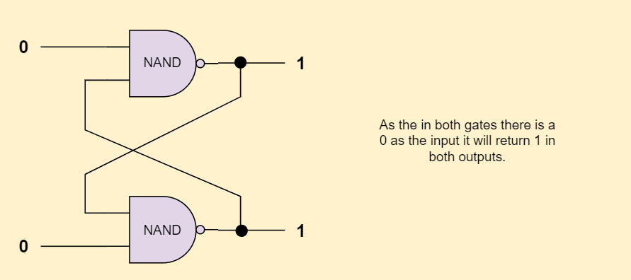
Figure 5: The Invalid State
Case 4: Hold Condition
When both inputs are high (1), the outputs depend on the latch's previous state rather than the current inputs. This is known as the Hold condition, where Q and Q-bar remain unchanged, preserving the last valid state of the latch. For some applications, it is important to be able to maintain the latched state for long periods of time without modification, such as memory storage cells where data integrity is of high importance.
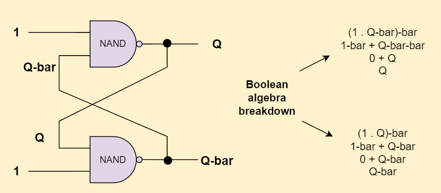
Figure 6: The Hold State
S-R Latch with a Truth Table
This table isn't just a theoretical tool but it's also practical for both circuit designers and students. It helps them see how the latch behaves under many conditions. Below, we present the comprehensive truth table for the SR Latch, followed by explanations and practical insights for each condition.
|
S |
R |
Q |
Q-BAR |
STATE |
|
0 |
0 |
1 |
1 |
Invalid |
|
0 |
1 |
0 |
1 |
Reset |
|
1 |
0 |
1 |
0 |
Set |
|
1 |
1 |
Q |
Q-bar |
Hold |
Chart 1: SR
Latch Truth Table
Explanation of Each Row
Set Condition (S = 1, R = 0): This row shows that when S is high and R is low, Q is set to high (1) and Q-bar to low (0). This mirrors the circuit's response to a set command, effectively storing a '1'.
Reset Condition (S = 0, R = 1): Here, the inputs indicate a reset operation. Consequently, Q is reset to low (0) and Q-bar is set to high (1). This state demonstrates the latch's capacity to revert to a '0'.
Invalid Condition (S = 0, R = 0): Both outputs become high in this condition, which is generally avoided because it results in both outputs being identical. This can lead to instability or undefined behavior in the latch, as it violates the rule that Q and Q-bar should always be opposites.
Hold Condition (S = 1, R = 1): In this scenario, the latch maintains its previous state, showcasing its ability to hold the last set state unless explicitly commanded to change.
Practical Insights and Tips
Understanding Outputs: Always remember that Q and Q-bar are ideally complements. Any deviation from this rule (as seen in the invalid condition) indicates a problem or misconfiguration.
Avoiding the Invalid State: It is imperative that designers take care to prevent the situation in which S and R are both low. Implementing additional logic or interlocks can help prevent this state.
Utilizing the Hold Condition: The hold condition can be particularly convenient in applications requiring data preservation over time. Maintaining data integrity may depend on making sure the latch does not inadvertently go into the set or reset state.
Interpreting the Truth Table: When designing or debugging circuits, reference the truth table to predict how changes in input will affect the output, especially in complex circuits where multiple latches are used.
Functional Dynamics of the S-R Latch
The S-R (Set-Reset) latch works well only if its inputs are managed correctly. To understand how it functions, you need to know how different input combinations affect the outputs, Q and Q-bar (the opposite of Q).
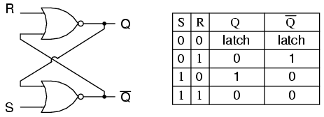
Figure 7: S-R Latch
If both Set (S) and Reset (R) are activated at the same time (S = 1 and R = 1), the latch goes into a "forbidden state," where both outputs, Q and Q-bar, are 0. This is a problem because normally, Q and Q-bar should be opposites.
Under normal conditions, to set the latch, you activate S (set S to 1) and deactivate R (set R to 0). This makes Q go high (1) and Q-bar go low (0), showing the latch can store a 1. To reset the latch, you activate R (set R to 1) and deactivate S (set S to 0). This makes Q go low (0) and Q-bar go high (1), showing the latch can clear itself and store a 0.
When both inputs are deactivated (S = 0 and R = 0), the latch keeps its last state, either set or reset. This is good for storing data or keeping a state without needing continuous input.
Race conditions can complicate the S-R latch's operation. These errors happen when the outputs rely heavily on the timing of input changes, leading to unpredictable results if the inputs change at nearly the same time. To prevent this and ensure the latch works reliably, time-delay mechanisms are often used. These delays make sure one input activates after the other has had time to stabilize. For the latch to be used in digital circuits where precise timing is required, it must perform consistently and maintain steady outputs. This is made possible by the controlled timing.
Logic Diagram of S-R Latch
The SR latch is a basic sequential logic circuit with two main configurations: NOR or NAND gates. Each setup affects how the latch works and responds to inputs, allowing customization for different electronic applications.
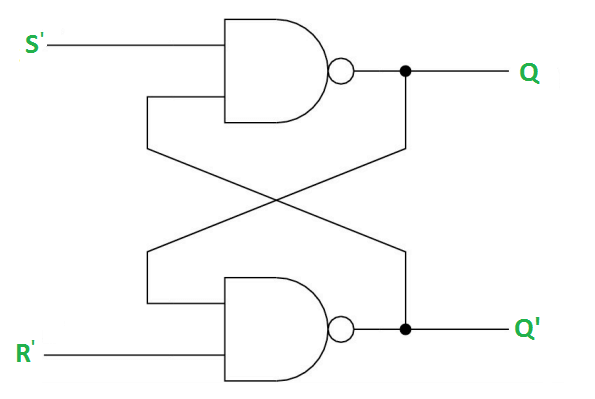
Figure 8: Logic Diagram Represents The S-R Latch Using NAND Gate
Implementation Using NAND Gates
When building an SR latch with NAND gates, a feedback loop is used to maintain its state. This setup allows the latch to keep its previous state when both inputs (S and R) are low. NAND gates output high unless both inputs are high. The state of the latch changes when one input is high and the other is low. It's best to avoid setting both S and R high at the same time because this forces both outputs to go low, leading to an undefined state where the outputs are no longer complementary. Proper input management is a must to prevent instability in NAND-based SR latches.
Implementation Using NOR Gates
Using NOR gates for an SR latch changes the operational conditions compared to NAND gates. In this configuration, the latch holds its state when both inputs are high. The latch changes state when one input is low and the other is high. NOR gates output high only if both inputs are low. This setup is useful in circuits where the default state is to have both outputs low, ensuring predictable output under high-input conditions. However, it's best to avoid setting both inputs low at the same time, as this causes conflicting outputs and reduces the latch's reliability.
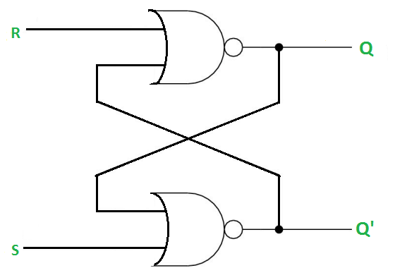
Figure 9: Logic Diagram Represents S-R Latch Using NOR Gate
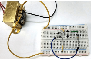
Example Circuit
Exploring how SR latches work in real life shows their usefulness. A good example is a circuit using the CD4001 chip, which has four NOR gates. This circuit shows how SR latches can control devices like LEDs with simple actions like pressing buttons.
In this example, the NOR gates in the CD4001 chip are set up to make an SR latch. Two gates are connected in a feedback loop to keep the latch state. Pushbuttons are added to the circuit as inputs for Set and Reset. Pressing a button changes the state of the input, which changes the latch and the LED state. For example, pressing the Set button lights up the LED, and it stays lit even after the button is released, showing how the latch can keep a state.
To make the circuit better, more LEDs can be added to show the output state of both Q and Q-bar. This makes it easier to see how the latch works, which is very helpful in learning environments.

Figure 10: S-R Latch Using The CD4001 Chip
Code Implementation
Translating the operational logic of an SR latch into software shows how digital logic design can work both in hardware and in virtual simulations. Using a programming language like C++ is effective because it supports the complex logic and control needed to imitate hardware behaviors.
To make an SR latch in C++, you start by defining the basic logic gates as functions that act like their hardware versions. For instance, a NAND gate function would return the opposite of the AND operation on its inputs. Similarly, a NOR gate function would return the opposite of the OR operation. With these basic functions, you can model the SR latch’s behavior by creating a feedback loop between these gate functions, based on the latch's circuit diagram.
The code would typically have a loop that continuously checks the states of the inputs (Set and Reset) and updates the outputs (Q and Q-bar) accordingly. Conditional statements inside this loop determine how changes in input affect the outputs, closely imitating the SR latch's physical behavior. For example, if both Set and Reset inputs are low, the outputs stay the same. If Set is high and Reset is low, output Q becomes high and Q-bar becomes low, replicating the latch's Set condition.
Here's a simple example of how this might look in code:
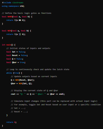
Figure 11: SR latch in C++
This code sets up a simple SR latch using NOR gates and continuously checks and updates the latch state based on the inputs.
Applications of the SR Latch
Control Systems in Motor Operations: The SR latch required by systems for motor control. Using start (S) and stop (R) pushbutton switches, the SR latch keeps a motor running even after the start button is released. This setup ensures the motor runs continuously until stopped, enhancing safety and convenience.
Memory and Data Storage: When creating larger memory circuits, the SR latch plays a role since it can store a single bit of data. It maintains data in a stable state until updated, forming the basis of memory cells in digital computing.
Signal Control and Management: In control signal applications, SR latches hold specific bits until certain conditions are met, ensuring proper sequence and timing in operations. Precision in signal processing and data flow depend on this.
Debouncing Circuits: SR latches stabilize signals from mechanical switches and buttons, preventing false triggering and errors caused by the "bounce" when switches are pressed. This is particularly fit in digital interfaces like keyboards.
Foundational Elements in Digital Systems: The design of flip-flops and counters, which are suitable for timing and sequencing in electronics, relies heavily on SR latches. They are also used as pulse latches for rapid state toggling.
Specialized Applications: In asynchronous systems, variations like the D latch are used for secure and reliable data transfer. In synchronous two-phase systems, data latches reduce transit count, improving efficiency and reducing delay.
Broader Implications in Electronics: SR latches are widely used in power gating circuits, playing a part in energy conservation within electronic devices. They manage power states at a detailed level, contributing to the overall energy efficiency of digital systems.
Conclusion
The S-R latch shows the importance of simple logic structures in complex digital systems. By looking at its different setups and how it works, we see that the S-R latch keeps data stable and makes systems efficient and reliable. It can work under various conditions, shown by truth tables and logic diagrams, making it adaptable for several uses, from motor control to basic digital circuits like flip-flops and counters. The S-R latch is suitable in many practical applications, such as memory cells in computers and debouncing circuits in digital interfaces, enhancing efficiency and reducing errors in electronic devices. With feedback mechanisms and careful input signal management, the S-R latch is good for designing more reliable and efficient digital systems. Studying its function through software simulations helps connect theoretical electronics with real-world applications, making the S-R latch an important topic for both new and experienced electronic engineers.
Frequently Asked Questions [FAQ]
1. What is the purpose of the SR latch?
The SR latch is used to store a single bit of data; it is a basic form of memory in digital circuits. Its main function is to retain the state of a bit until it is changed by input signals.
2. Is SR latch active high or low?
The SR latch is typically active high, meaning it responds to high inputs (logic level 1). When the inputs S (Set) and R (Reset) are high, they trigger changes in the output.
3. What is the disadvantage with an SR latch?
A major drawback of the SR latch is its susceptibility to an invalid condition where both the Set and Reset inputs are high simultaneously. This situation leads to an undefined output, which can result in unreliable or unpredictable behavior.
4. What are the rules for the SR latch?
If S (Set) is high and R (Reset) is low, the output Q is set to high.
If R is high and S is low, the output Q is reset to low.
If both S and R are low, the output retains its previous state.
If both S and R are high, the output is undefined or invalid.
5. What is memory in SR latch?
The memory in an SR latch refers to its ability to maintain the output state (high or low) indefinitely, until it receives input to change the state. This makes it a bistable device, ideal for simple memory storage.
6. What are the outputs of the SR latch?
The SR latch has two outputs, Q and Q' (Q-bar). Q represents the current state, while Q' is the inverse of Q. When Q is high, Q' is low, and vice versa.
7. Where do we use latch?
When short-term data storage or state retention are required, latches are employed in different kinds of applications. This includes data storage in flip-flops, registers, and memory units, as well as in systems requiring data synchronization and circuit hold functions.
About us
ALLELCO LIMITED
Read more
Quick inquiry
Please send an inquiry, we will respond immediately.
Static Electricity
on June 19th
The Backbone of Electrical Systems: A Comprehensive Guide to Rectifiers
on June 17th
Popular Posts
-
What is GND in the circuit?
on January 1th 2933
-

RJ-45 Connector Guide: RJ-45 Connector Color Codes, Wiring Schemes, R-J45 Applications, RJ-45 Datasheets
on January 1th 2494
-

Fiber Connector Types: SC Vs LC And LC Vs MTP
on January 1th 2083
-
Understanding Power Supply Voltages in Electronics VCC, VDD, VEE, VSS, and GND
on November 8th 1884
-

Comparison Between DB9 and RS232
on January 1th 1759
-

What Is An LR44 Battery?
Electricity, that ubiquitous force, quietly permeates every aspect of our daily lives, from trivial gadgets to life-threatening medical equipment, it plays a silent role. However, truly grasping this energy, especially how to store and efficiently output it, is no easy task. It is against this background that this article will focus on a type of coin cell battery that may seem insignificant on the...on January 1th 1710
-
Understanding the Fundamentals:Inductance Resistance, andCapacitance
In the intricate dance of electrical engineering, a trio of fundamental elements takes center stage: inductance, resistance, and capacitance. Each bears unique traits that dictate the dynamic rhythms of electronic circuits. Here, we embark on a journey to decipher the complexities of these components, to uncover their distinct roles and practical uses within the vast electrical orchestra. Inductan...on January 1th 1651
-

CR2430 Battery Comprehensive Guide: Specifications, Applications and Comparison to CR2032 Batteries
What is CR2430 battery ?Benefits of CR2430 BatteriesNormCR2430 Battery ApplicationsCR2430 EquivalentCR2430 VS CR2032Battery CR2430 SizeWhat to look for when buying the CR2430 and equivalentsData Sheet PDFFrequently Asked Questions Batteries are the heart of small electronic devices. Among the many types available, coin cells play a crucial role, commonly found in calculators, remote controls, and ...on January 1th 1541
-
What Is RF and Why Do We Use It?
Radio Frequency (RF) technology is a key part of modern wireless communication, enabling data transmission over long distances without physical connections. This article delves into the basics of RF, explaining how electromagnetic radiation (EMR) makes RF communication possible. We will explore the principles of EMR, the creation and control of RF signals, and their wide-ranging uses. The article ...on January 1th 1537
-

CR2450 vs CR2032: Can The Battery Be Used Instead?
Lithium manganese batteries do have some similarities with other lithium batteries. High energy density and long service life are the characteristics they have in common. This kind of battery has won the trust and favor of many consumers because of its unique safety. Expensive tech gadgets? Small appliances in our homes? Look around and you'll see them everywhere. Among these many lithium-manganes...on January 1th 1504
HOT Part Number
-

MOC8204SM
onsemi
OPTOISO 4.17KV TRANS W/BASE 6SMD
VI-MU4-ES
Vicor Corporation
AC/DC CONVERTER 48V 300W
MAX3374EEKA
Analog Devices Inc./Maxim Integrated
MAX3374EEKA
IRU1206-25CYTR
Infineon Technologies
IC REG LINEAR 2.5V 1A SOT223
NE94433-T1B
CEL
RF TRANS NPN 15V 2GHZ SOT23
R43160
Microchip Technology
DIODE GP 1.6KV 150A DO205AA
AP2151AFM-7
Diodes Incorporated
IC PWR SWITCH P-CHAN 1:1 6UDFN
TXB0108PWR
Texas Instruments
IC TRANSLATOR BIDIR 20TSSOP
CDCEL925PW
Texas Instruments
IC CLK/FREQ SYNTH 16TSSOP
1761008-1
TE Connectivity AMP Connectors
CONN SFP CAGE 1X4 PRESS-FIT R/A
P6SMBJ200CA
Littelfuse Inc.
TVS DIODE 171VWM 274VC DO214AA
STTH60L06CW
STMicroelectronics
DIODE ARRAY GP 600V 40A TO247-3
12103D475MAT2A
KYOCERA AVX
CAP CER 4.7UF 25V X5R 1210
APXA100ARA560MF55G
United Chemi-Con
CAP ALUM POLY 56UF 20% 10V SMD
GRM0335C1H6R3CA01D
Murata Electronics
CAP CER 6.3PF 50V C0G/NP0 0201
W9812G6JB-6I
Winbond Electronics
IC DRAM 128MBIT PAR 54TFBGA
Z8F3222AR020SC
Zilog
IC MCU 8BIT 32KB FLASH 64LQFP
CSD68832L
Texas Instruments
PROTOTYPE -
SN75LVDS388ADBT
Texas Instruments
IC RECEIVER 0/8 38TSSOP
DF13-10P-1.25H(21)
Hirose Electric Co Ltd
CONN HEADER SMD R/A 10POS 1.25MM
HEDS-9100#E00
Broadcom Limited
ROTARY ENCODER OPTICAL 200PPR
MAX267BCNG+
Analog Devices Inc./Maxim Integrated
IC FILTER 57KHZ BAND PASS 24DIP
12063A472GAT4A
KYOCERA AVX
CAP CER 4700PF 25V C0G/NP0 1206
SD3118-3R3-R
Eaton - Electronics Division
FIXED IND 3.3UH 1.22A 113MOHM SM
7024S15PF
Renesas Electronics America Inc
IC SRAM 64KBIT PARALLEL 100TQFP
TAJA226K006RNJ
KYOCERA AVX
CAP TANT 22UF 10% 6.3V 1206
LTC6406IUD#TRPBF
Analog Devices Inc.
IC ADC DRIVER 16QFN
C4532CH2W473J230KA
TDK Corporation
CAP CER 0.047UF 450V CH 1812
SN74AUC07RGYRG4
Texas Instruments
IC BUFFER NON-INVERT 2.7V 14VQFN
TPSM828214SILR
Texas Instruments
5.5-V INPUT, 1-A STEP-DOWN MODUL
XCR3512XL-10FT256I
AMD
IC CPLD 512MC 9NS 256FTBGA
NSV9435T1G
onsemi
PNP BIPOLAR DIGITAL TRANSISTOR (
SI3865DDV-T1-GE3
Vishay Siliconix
IC PWR SWITCH P-CHAN 1:1 6TSOP
LPC11E67JBD64E
NXP USA Inc.
IC MCU 32BIT 128KB FLASH 64LQFP
MRF373ALR1
NXP USA Inc.
FET RF 70V 860MHZ NI-360
744043330
Würth Elektronik
FIXED IND 33UH 820MA 230MOHM SMD -

CL21B473KBANNNC
Samsung Electro-Mechanics
CAP CER 0.047UF 50V X7R 0805
MX29GL640ELXFI-70G
Macronix
IC FLASH 64MBIT PARALLEL 64LFBGA
DAC0800LCMX
Texas Instruments
IC DAC 8BIT A-OUT 16SOIC
OPA2348AIDGK
Texas Instruments
IC CMOS 2 CIRCUIT 8VSSOP
LP2981AIM5-5.0
Texas Instruments
IC REG LINEAR 5V 100MA SOT23-5
HMC392ALC4
Analog Devices Inc.
IC AMP CDMA 3.5GHZ-8GHZ 24CLCC
CD4022BPWR
Texas Instruments
IC BINARY COUNTER 4-BIT 16TSSOP
TOP261LN
Power Integrations
IC OFFLINE SWITCH FLYBACK 7FESIP
IXGQ200N30PB
IXYS
IGBT 300V 400A TO3P
CAT24WC04L
Catalyst Semiconductor Inc.
IC EEPROM 4KBIT I2C 400KHZ 8DIP
PIC16LC62B-04/SO
Microchip Technology
IC MCU 8BIT 3.5KB OTP 28SOIC
TM11R-5M2-88
Hirose Electric Co Ltd
CONN MOD JACK 8P8C R/A SHIELDED
1N1184RA
Solid State Inc.
DIODE GEN PURP REV 12A DO4
MAX355CWE+
Analog Devices Inc./Maxim Integrated
IC SWITCH SP4T X 2 350OHM 16SOIC
SN74LS541N
Texas Instruments
IC BUF NON-INVERT 5.25V 20DIP
S-80848CNMC-B89T2G
ABLIC Inc.
IC SUPERVISOR 1 CHANNEL SOT23-5
S-1133B33-U5T1G
ABLIC Inc.
IC REG LINEAR 3.3V 300MA SOT89-5
1N4003RLG
onsemi
DIODE GEN PURP 200V 1A AXIAL