Understanding MOSFET: Types, Working Principles, and Applications
MOSFETs is tiny yet powerful components of modern electronics, making everything from smartphones to power supplies work efficiently. If you're new to electronics or looking to deepen your understanding, this guide is perfect for you. We'll break down the basics of MOSFETs, explaining how they work, the different types available, and how to choose the right one for your project. We'll also explore their many applications and discuss the pros and cons of using them. Let's discover how MOSFETs can transform your electronic creations!Catalog
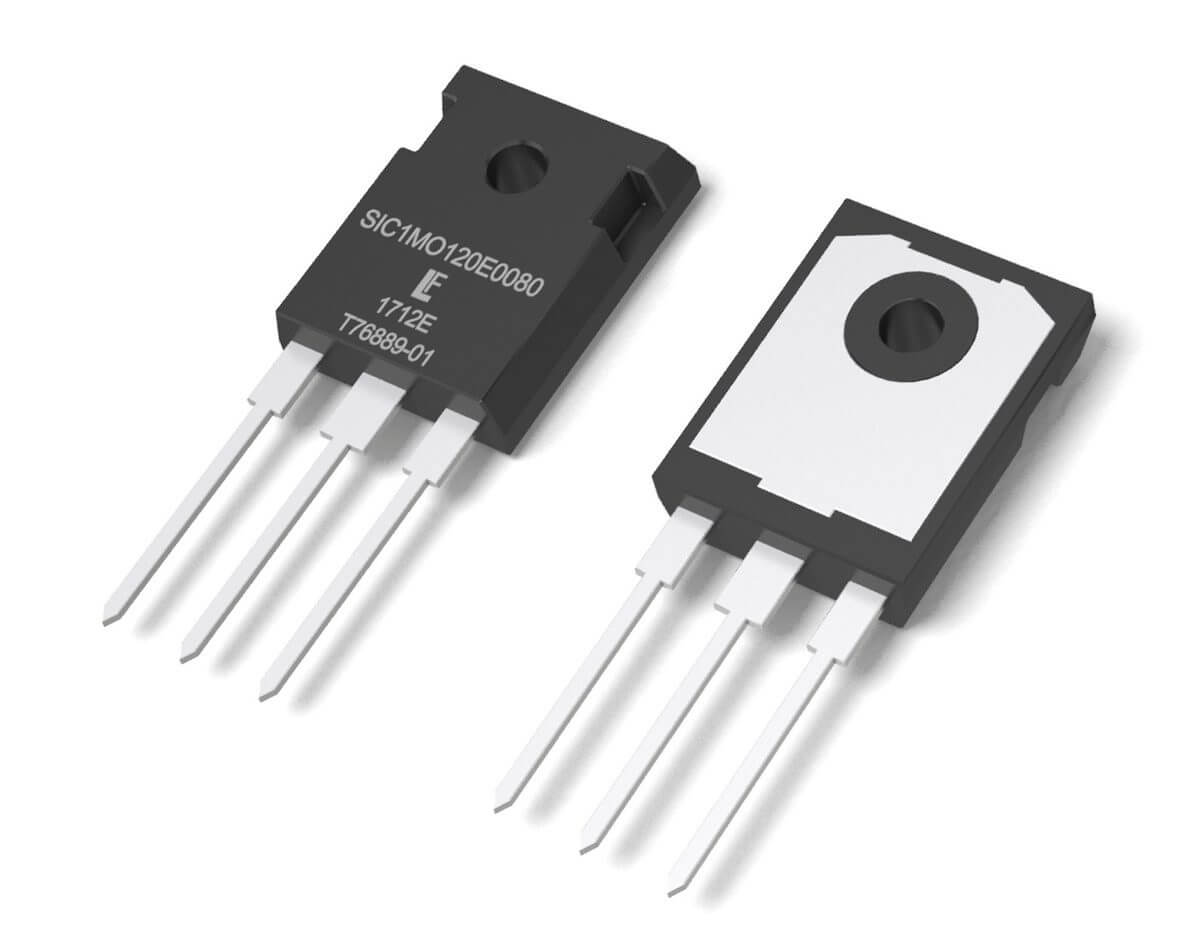
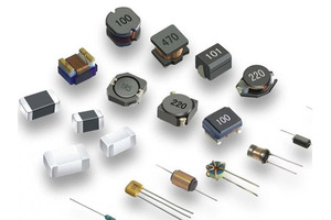
Figure 1: MOSFETs
Introduction to MOSFETs
A MOSFET, or Metal Oxide Semiconductor Field Effect Transistor, is a type of transistor designed to overcome the limitations of traditional Field Effect Transistors (FETs). These limitations include high drain resistance, moderate input impedance, & slower speeds. MOSFETs offer an advanced and more efficient form of FET technology. They are also known as Insulated Gate Field Effect Transistors (IGFETs) due to the insulation characteristic of their gate structure. MOSFETs are voltage-controlled devices; applying a specific voltage to the gate pin allows them to conduct electrical current between the drain and source pins.
The main difference between FETs and MOSFETs lies in the construction of the gate electrode. In a MOSFET, the gate electrode is made of metal oxide and is electrically insulated from the semiconductor channel by a thin layer of silicon dioxide or glass. This insulation increases the input resistance of the MOSFET, often reaching mega-ohms (MΩ). This high input resistance makes MOSFETs effective in many applications.
Common MOSFET packages include the TO-220, known for its robust performance and ease of handling. Popular models such as the IRFZ44N, BS170, IRF520, and 2N7000 are favored in various applications due to their reliable performance & suitability for different environments.
How a MOSFET Works?
The working principle of a MOSFET is to act as an efficient electronic switch, controlling the voltage and current flow between the source and drain terminals. The key part of this operation is the MOS capacitor, which changes from p-type to n-type when you apply specific gate voltages. This change allows the MOSFET to manage the current flow precisely.
To operate a MOSFET, you apply a voltage between the drain and source terminals (VDS). A positive voltage on the drain and a negative voltage on the source initially stop current from flowing. When you apply a positive voltage to the gate terminal, it attracts electrons in the P-type substrate to the gate area. This forms a conductive channel between the N-type regions (drain and source). Increasing the positive gate voltage attracts more electrons, widening the N-channel and allowing more current (ID) to flow. The MOSFET starts to conduct at a specific voltage called the threshold voltage.
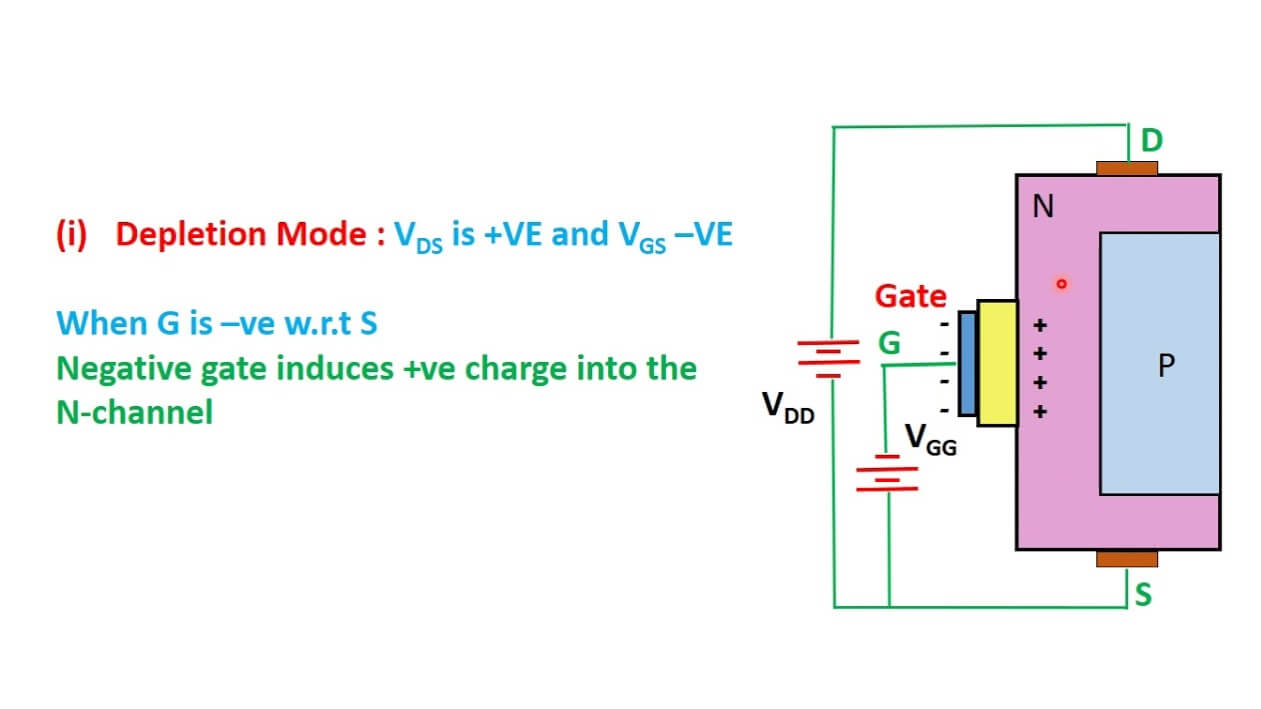
Figure 2: Depletion Mode Operation
In depletion-mode MOSFETs, the channel is open without any gate voltage, so current flows freely between the source and drain. These are often called "Switched ON" devices. When you apply a positive gate voltage, the channel widens, and more current (ID) flows. If you apply a very negative gate voltage, the channel narrows, reducing the current flow and potentially stopping it completely. The voltage-current (V-I) characteristics of depletion-mode MOSFETs show the drain-source voltage (VDS) on the horizontal axis and the drain current (ID) on the vertical axis. With no gate voltage, the MOSFET conducts very well. A positive gate voltage increases the channel width and the drain current, while a negative gate voltage decreases the channel width and the drain current.
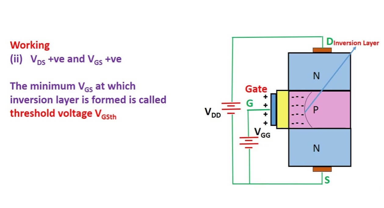
Figure 3: Enhancement Mode Operation
Enhancement-mode MOSFETs act like an open switch. They only conduct when a positive voltage (+VGS) is applied to the gate terminal. This positive voltage is needed to create a conductive channel between the drain and source. As the gate voltage increases, the channel widens, and more current (ID) flows. Without gate voltage, the MOSFET stays OFF, and no current flows between the source and drain.
The VI characteristics for enhancement-mode MOSFETs show drain current (ID) on the vertical axis and drain-source voltage (VDS) on the horizontal axis. In the cutoff region, with no gate voltage, the MOSFET is OFF, and no current flows. In the ohmic region, with gate voltage, the MOSFET conducts, and current increases linearly with voltage, acting like a variable resistor. In the saturation region, further increases in VDS do not significantly increase ID, and the MOSFET stays in a conductive state with constant current flow, which is good for switching applications.
Different Types of MOSFETs
Types of MOSFETs by Operational Modes
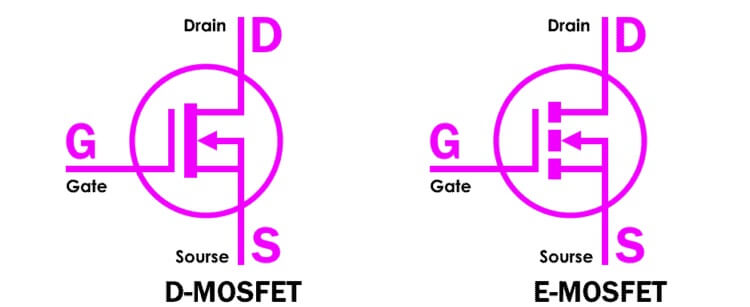
Figure 4: Depletion Mode and Enhancement Mode
Depletion Mode MOSFETs (D-MOSFETs) - Unlike E-MOSFETs, D-MOSFETs are normally on when the gate-source voltage is zero. Applying a negative gate-source voltage for N-channel D-MOSFETs or a positive gate-source voltage for P-channel D-MOSFETs turns the device off. These transistors are often utilized in analog circuits where a normally-on condition is beneficial.
Enhancement Mode MOSFETs (E-MOSFETs) - In these MOSFETs, the transistor remains off when the gate-source voltage (V_GS) is zero. To turn the device on, a positive gate-source voltage is applied for N-channel E-MOSFETs, or a negative gate-source voltage for P-channel E-MOSFETs. This type is widely used due to its high input impedance and low power consumption, making it ideal for digital circuits.
Types of MOSFETs by Channel Type
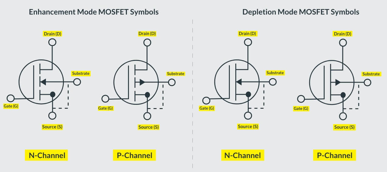
Figure 5: Types of MOSFETs by Channel Type
MOSFETs are further classified by the type of channel they use, resulting in four primary variations:
N-Channel Enhancement Mode MOSFET - This type requires a positive gate-source voltage to induce a conductive channel between the source and drain. They are widely used due to their efficient switching capabilities and are common in power applications & digital circuits.
P-Channel Enhancement Mode MOSFET - In this variation, a negative gate-source voltage is needed to create a conductive channel. P-channel E-MOSFETs are often used in scenarios where a positive supply voltage needs to be switched, and they are frequently paired with N-channel MOSFETs in push-pull amplifier stages.
N-Channel Depletion Mode MOSFET - This kind has a conductive channel present when no voltage is applied to the gate. It requires a negative gate-source voltage to deplete the channel and turn the device off. N-channel D-MOSFETs are known for their higher electron mobility compared to P-channel counterparts, which allows for better performance in high-speed applications.
P-Channel Depletion Mode MOSFET - In this type, a conductive channel is also present when no voltage is applied to the gate. However, it requires a positive gate-source voltage to turn off. P-channel D-MOSFETs are typically used in complementary configurations with N-channel devices to create CMOS (Complementary MOS) logic circuits.
MOSFET by Mount Types
Panel Mounted - Panel-mounted MOSFETs are screwed onto metal plates or heat sinks. It handles high current applications with excellent thermal management. That ensure efficient operation under heavy loads.
PCB Mounted - PCB-mounted MOSFETs fit securely onto printed circuit boards, often with tabs to prevent incorrect fitting and protect against overcurrent conditions. This mounting is common in consumer electronics & industrial applications.
Surface Mounted - Surface-mounted MOSFETs offer quick and reliable assembly onto PCBs. This MOSFETs is ideal for compact and high-density applications. Extensively used in modern electronics due to their ease of integration and dependable performance.
Through Hole Mounted - Through-hole mounted MOSFETs provide strong mechanical bonds by inserting component leads through PCB holes. This method is preferred for large and heavy components. That guarantee durability in high-power and industrial applications.
Key Components of a MOSFET
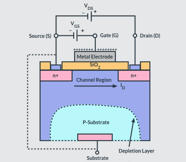
Figure 6: Structure of a MOSFET
Building MOSFETs is a big improvement over older FET design. To understand how MOSFETs work and why they are effective in today's electronics, it's important to know their internal structure.
A typical MOSFET has several important parts:
Gate Terminal - The most critical element, located on a thin metal layer. It is insulated from the main semiconductor material by a silicon dioxide (SiO2) layer, preventing direct electrical contact.
Source - The source is a terminal where carriers (electrons or holes) enter the MOSFET. It acts as the entry point for these charge carriers flowing through the device.
Drain - The drain is the terminal where carriers leave the MOSFET. It acts as the exit point for the charge carriers. The movement of carriers from the source to the drain creates the current that flows through the MOSFET.
Gate - The gate is a terminal that controls the flow of carriers between the source and drain. It is separated from the channel by a thin insulating layer (usually silicon dioxide). When you apply a voltage to the gate, it creates an electric field that controls how easily the current can flow through the channel. This way, the gate regulates the current flow.
Substrate (Body) - The substrate, also called the body, is the main part of the MOSFET. It is usually made of silicon and can be either p-type or n-type. The substrate is connected to the source terminal, either inside the MOSFET or outside. It can affect the voltage needed to turn the MOSFET on.
Oxide Layer - The oxide layer is a thin insulating layer (usually silicon dioxide) between the gate and the channel. This layer stops direct current from flowing between the gate and the channel. Instead, it lets the gate control the channel using an electric field.
Channel Region - This is where conduction happens. It has two N-type semiconductor regions at the drain and source terminals, with the channel also made of N-type material. The surrounding substrate is made of P-type material, which creates the right conditions for the MOSFET to work effectively.
MOSFET Operating Regions
• Cut-Off Region
In the cut-off region, the MOSFET acts like an open switch and does not conduct any current between the drain and source terminals. In this state, the gate-source voltage (VGS) is below the threshold voltage, so no conductive channel forms. Without this channel, the MOSFET remains non-conductive, and no current flows through it. This region is important for digital logic circuits and other applications where the MOSFET needs to act as an on-off switch, isolating the load from the power source when it is off.
• Ohmic Region
The ohmic region, also called the linear region, is where the MOSFET acts like a variable resistor. In this region, the current (ID) flowing through the MOSFET increases linearly with the drain-source voltage (VDS). The gate-source voltage (VGS) is above the threshold voltage, so a conductive channel forms between the drain and source. As the gate voltage increases, the channel's resistance decreases, allowing more current to flow for a given VDS. This makes the MOSFET useful for analog applications, like amplifiers, where precise control of current is needed. In these cases, the MOSFET can amplify small input signals by changing the output current in proportion to the input voltage.
• Saturation Region
In the saturation region, the MOSFET acts as a constant current source. Here, the drain current (ID) stays mostly the same even if the drain-source voltage (VDS) increases. This happens because the channel between the drain and source is fully open, so more VDS doesn't change the current much. The MOSFET works like a closed switch in this region, giving a steady current flow. This is great for switching operations. In power electronics, like switching power supplies or motor controllers, the MOSFET often works in the saturation region to ensure steady performance and efficient power delivery.
MOSFET Packaging Options
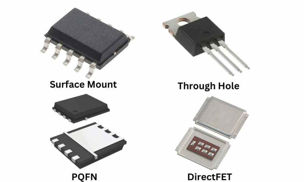
Figure 7: MOSFET Packaging Options
MOSFETs come in different packages to meet various application needs.
The choice of package affects performance, handling, and suitability for
specific uses. Below are the different packaging types and their common
applications:
Surface Mount Packages
Surface mount packages are compact and offer efficient heat dissipation. They are directly mounted on the surface of printed circuit boards (PCBs), making them ideal for high-density and automated manufacturing processes. Examples include TO-263, which is low profile with excellent heat dissipation and commonly used in power supplies. TO-252 (DPAK) has a smaller footprint and is popular in automotive and industrial applications. MO-187 is suitable for power management and audio applications. SO-8 is ideal for battery-powered devices and portable electronics. SOT-223 provides good thermal performance and is often used in voltage regulation. SOT-23 is one of the smallest packages, used where space is limited. TSOP-6 is a thin small outline package used in compact consumer electronics.
Through-Hole Packages
Through-hole packages are used where strong mechanical bonds and easy hand soldering are needed. These packages feature leads that go through PCB holes, offering durability & reliability. Examples include TO-262, used in power transistors and voltage regulators. TO-251 is smaller than TO-262 and used in medium power applications. TO-274 is known for high power handling capability. TO-220 is a popular package with excellent heat dissipation and ease of mounting. It is used in a wide range of applications from power supplies to motor controllers. TO-247 is larger than TO-220, providing enhanced power handling & thermal management for high-power applications.
PQFN (Power Quad Flat No-lead) Packages
PQFN (Power Quad Flat No-lead) packages are designed for high-efficiency power management with excellent thermal performance. They are suitable for compact, high-performance applications. Examples include PQFN 2x2, ideal for portable devices requiring minimal space and efficient power management. PQFN 3x3 balances size and power handling and is used in consumer electronics. PQFN 3.3x3.3 is slightly larger for improved thermal performance in medium power applications. PQFN 5x4 is suitable for higher power applications with good thermal dissipation. PQFN 5x6 is one of the largest PQFN packages, used in high-power & high-efficiency applications like computing and telecommunication equipment.
DirectFET Packages
DirectFET packages are designed for optimal thermal and electrical performance. Often used in high-performance computing and power management applications. These packages eliminate traditional wire bonds, reducing resistance and improving efficiency. Variations like DirectFET M4, MA, MD, ME, S1, and SH offer different sizes and power handling capabilities. They are tailored for specific high-performance applications. The DirectFET design allows for excellent heat dissipation and high current handling. Suitable for demanding applications such as servers, laptops, and high-efficiency power supplies.
Selecting the Right MOSFET for Your Project
Selecting the appropriate MOSFET for your project involves a careful assessment of your specific requirements and the characteristics of various MOSFETs available in the market. Although this task can appear complex, simplifying it into key considerations makes the process more approachable. Understanding the fundamental distinctions between N-channel and P-channel MOSFETs, voltage and current ratings, gate parameters, and other attributes will guide you toward the best choice for your application.
N-Channel vs. P-Channel
The first step in selecting a MOSFET is deciding whether an N-channel or P-channel MOSFET suits your needs. N-channel MOSFETs are more efficient and widely used because they conduct when a positive voltage is applied to the gate relative to the source. Thus, they are ideal for low-side switching. On the other hand, P-channel MOSFETs conduct when a negative voltage is applied to the gate relative to the source. Due to that, they suit for high-side switching applications. This difference influences the overall efficiency and performance of your circuit.
Voltage and Current Ratings
For dependable operation, you need to ensure MOSFET’s voltage and current ratings exceed the maximum values in your circuit. The Drain-Source Voltage (VDS) rating should be higher than the peak voltage in your circuit to prevent breakdowns, while the Gate-Source Voltage (VGS) must be compatible with the driving voltage from your control circuitry. Aside from that, the Drain Current (ID) rating should comfortably handle the maximum current your application will draw, with an added safety margin for potential surges. This guarantee that the MOSFET operates within safe limits. That will prevent overheating and potential failure.
Gate Parameters and Technology Impact
The gate parameters of a MOSFET are need to consider to make sure efficient operation with your driver circuitry. The Gate Threshold Voltage (VGS(th)), which is the voltage needed to start turning the MOSFET on, must be within the range that your driver can supply. Besides, a lower Gate Charge (Qg) is desirable for faster switching and reduced power consumption, especially in high-speed applications.
Also consider the MOSFET's construction technology; Trench MOSFETs, for example, offer lower on-resistance and higher current handling compared to Planar MOSFETs, while Super Junction Technology provides enhanced efficiency for high-voltage applications.
Finally, proper thermal management is need to consider, such as adequate heat sinks or cooling solutions. It is required for maintaining safe junction temperatures and ensure longevity in high-power applications.
Common Uses of MOSFETs
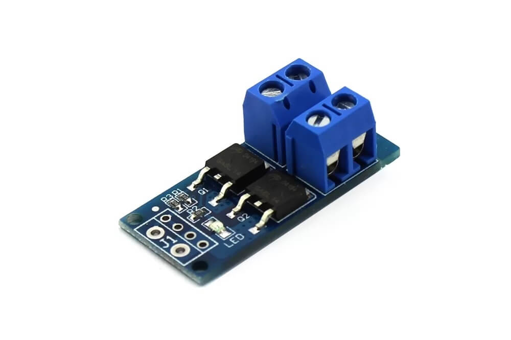
Figure 8: Applications of MOSFET
MOSFETs are versatile components used to switch or amplify electrical signals by altering their conductivity in response to an applied voltage. They are found in millions within memory chips, microprocessors, pocket calculators, digital wristwatches, etc.
MOSFET as a Switch
MOSFETs efficiently control large currents with small input voltages. For example, they can turn lamps on and off in circuits. A positive gate voltage turns the MOSFET on, allowing current to illuminate the lamp. A zero or negative gate voltage turns it off, stopping the current and extinguishing the lamp.
To optimize performance during fast switching, additional components like pull-down resistors and current-limiting capacitors are used. Pull-down resistors keep the gate voltage low when not driven high, preventing unintended switching. Current-limiting capacitors manage gate capacitance, reducing parasitic effects and improving switching speed. For inductive or capacitive loads, protective components like snubber circuits or freewheeling diodes prevent damage from high inrush currents or reverse voltages.
As switches, they handle varying voltage & current levels with minimal power loss and heat generation. This makes them ideal for audio equipment, signal processing, & other applications.
MOS Integrated Circuits
MOSFETs are utilized in producing integrated circuits (ICs). Unlike bipolar transistors, MOSFETs don't need P-N junction isolation. It simplifies manufacturing and allowing for high-density ICs production. This is important for creating microprocessors, memory chips, and other complex digital circuits.
CMOS Circuits
CMOS (Complementary Metal-Oxide-Semiconductor) technology uses both P-channel and N-channel MOSFETs to create highly efficient IC chips. CMOS circuits are used extensively in digital logic circuits due to their high noise immunity & low static power consumption. These features enable high-density logic functions with minimal heat generation.
Power Electronics
MOSFETs play a major role in power electronics, managing and converting power efficiently. They are used for battery protection, switching power sources, and managing loads in various devices. Their compact size, high current capacity, and built-in ESD protection make them stand out in power supplies, inverters, and telecommunication networks.
MOS Memory
MOSFETs are key in developing dynamic random-access memory (DRAM). They offer high performance, low power consumption, and cost-effectiveness compared to traditional magnetic core memory. Hence, they are perfect for a range of computing applications from personal computers to large data centers.
MOSFET Sensors
MOSFET sensors, or MOS sensors, measure various physical, chemical, biological, and environmental parameters. They are used in microelectromechanical systems (MEMS), interacting with and processing elements like chemicals, light, and movement. MOSFET technology is also used in image sensing, forming the basis for charge-coupled devices (CCDs) & active-pixel sensors in cameras and other imaging equipment.
Quantum Physics
Advanced MOSFETs, such as quantum field-effect transistors (QFETs) and quantum-well field-effect transistors (QWFETs), utilize quantum tunneling to enhance speed and performance. These devices rely on rapid thermal processing for efficient operation. Thus, they are ideal for quantum computing and other high-performance applications.
Advantages and Disadvantages of MOSFET
MOSFETs are integral to modern electronics due to their numerous benefits. However, they also come with drawbacks. Understanding these pros and cons can help designing circuits and selecting components effectively.
Advantages of MOSFET
High Switching Speed - MOSFETs can switch rapidly between on and off states. Due to that, they are ideal for applications that require fast and efficient switching, such as digital logic circuits and power supplies. Their high-speed capability improves efficiency in handling high-frequency signals.
Low Power Consumption - MOSFETs consume very little power, especially in idle states. This is particularly beneficial for battery-operated devices, as it extends battery life and reduces overall energy consumption. Their minimal power draw in the off state makes them suitable for energy-efficient applications.
High Input Impedance - MOSFETs have a very high input impedance, requiring minimal input current to operate. This reduces the load on preceding circuit stages, enhancing overall system efficiency & performance. High input impedance also improves signal integrity and reduces distortion in analog applications.
Low Noise Levels - MOSFETs generate low electrical noise. Thus, they are ideal for sensitive analog circuits where signal purity is needed. Their low noise characteristics ensure clearer and more accurate signal amplification and processing. That feature is required in audio and RF applications.
Cost-Effective Manufacturing - Advancements in semiconductor fabrication have made MOSFETs cost-effective. Although their initial manufacturing process is complex, the ability to produce them in large quantities using standard silicon wafer processing techniques has driven down costs. Their widespread availability also contributes to affordability. They are a budget-friendly option for designers and manufacturers.
High-Temperature Performance - MOSFETs perform well in high-temperature environments. Thus, they are ideal for industrial and automotive applications. Unlike BJTs, which can suffer from thermal runaway due to increased leakage currents at high temperatures, MOSFETs maintain stability and performance. This thermal stability is important for devices exposed to harsh conditions or requiring reliable operation at elevated temperatures.
Effective Voltage Amplification - MOSFETs excel in voltage amplification applications. They possess high input impedance and low output impedance. This makes them effective in amplifying weak signals without loading the preceding stage. With their two conducting terminals (drain and source), MOSFETs provide a straightforward and efficient means of voltage amplification compared to BJTs, which require a base-emitter junction to control current flow.
MOSFET Disadvantages
Susceptibility to Breakdown - MOSFETs have very thin gate oxide layers. Because of that, they are susceptible to breakdown under high voltage conditions. This thin layer, while improving performance, makes them vulnerable to electrostatic discharge (ESD) or excessive voltage. Careful handling and design considerations is need to consider for damage prevention.
Temperature Sensitivity - MOSFET performance can be affected by temperature changes. High temperatures can alter their operating characteristics. It can lead to reduced efficiency or failure. Effective thermal management strategies, such as heat sinks or active cooling, are necessary, especially in high-power applications.
Limited Voltage Capacity - MOSFETs have a limited voltage capacity compared to other transistors, such as Insulated-Gate Bipolar Transistors (IGBTs). This limitation makes them less ideal for very high-voltage applications without risking breakdown. Designers must choose MOSFETs with appropriate voltage ratings to guarantee reliable operation.
High Manufacturing Costs - The manufacturing processes for MOSFETs are complex and contribute to their higher cost compared to other transistors. This includes the precision needed to create thin gate oxide layers and the overall semiconductor fabrication process. Although costs have decreased with technological advancements, MOSFETs can still be more expensive than simpler transistor types, affecting the final product cost.
Conclusion
MOSFETs are key parts that make many of our modern electronic device work. They are incredibly useful because they can switch on and off quickly and use very little power. By learning about the different types of MOSFETs, how they work, and how to choose the right one, you can improve your electronic projects. Whether you’re working on a simple gadget or manufacturing complex system, understanding MOSFETs will help you create more efficient and reliable devices. With this knowledge, you can make your electronic projects better and more effective.
Frequently Asked Questions [FAQ]
1. How can I test a MOSFET?
To test a MOSFET, use a multimeter in diode mode. Check the gate-to-source junction by placing the positive probe on the gate and the negative on the source; there should be no reading. Charge the gate by placing the positive probe on the drain and the negative on the source; you should see a low resistance if the MOSFET is N-channel (high resistance for P-channel). Briefly touch the positive probe to the gate while keeping the negative probe on the source. Move the positive probe back to the drain; the resistance should remain low (or high for P-channel). Discharge the gate by touching it with a negative probe and recheck the resistance; it should show high resistance (or low for P-channel).
2. How do I interpret the numbers on a MOSFET?
The numbers on a MOSFET include the part number, voltage rating (Vds), current rating (Id), gate threshold voltage (Vgs(th)), and package type.
3. Are MOSFETs used with AC or DC power?
MOSFETs are typically used with DC power but can be used in circuits that handle AC signals, especially in applications like AC to DC converters.
4. What are common causes of MOSFET failure?
Common causes of MOSFET failure include overheating, overvoltage, overcurrent, electrostatic discharge (ESD), and improper gate drive.
5. Are MOSFETs cost-effective?
Yes, MOSFETs are cost-effective due to their high efficiency, fast switching speeds, and low power consumption. They are an economical choice for a wide range of applications. Advances in manufacturing have also reduced costs.
About us
ALLELCO LIMITED
Read more
Quick inquiry
Please send an inquiry, we will respond immediately.
Centrifugal Switch Guide - Types, Symbols, Operating Principles, and Applications
on May 30th
Driving Motion: A Comprehensive Guide to Actuators
on May 28th
Popular Posts
-
What is GND in the circuit?
on January 1th 2946
-

RJ-45 Connector Guide: RJ-45 Connector Color Codes, Wiring Schemes, R-J45 Applications, RJ-45 Datasheets
on January 1th 2502
-

Fiber Connector Types: SC Vs LC And LC Vs MTP
on January 1th 2091
-
Understanding Power Supply Voltages in Electronics VCC, VDD, VEE, VSS, and GND
on November 9th 1898
-

Comparison Between DB9 and RS232
on January 1th 1765
-

What Is An LR44 Battery?
Electricity, that ubiquitous force, quietly permeates every aspect of our daily lives, from trivial gadgets to life-threatening medical equipment, it plays a silent role. However, truly grasping this energy, especially how to store and efficiently output it, is no easy task. It is against this background that this article will focus on a type of coin cell battery that may seem insignificant on the...on January 1th 1714
-
Understanding the Fundamentals:Inductance Resistance, andCapacitance
In the intricate dance of electrical engineering, a trio of fundamental elements takes center stage: inductance, resistance, and capacitance. Each bears unique traits that dictate the dynamic rhythms of electronic circuits. Here, we embark on a journey to decipher the complexities of these components, to uncover their distinct roles and practical uses within the vast electrical orchestra. Inductan...on January 1th 1662
-
CR2430 Battery Comprehensive Guide: Specifications, Applications and Comparison to CR2032 Batteries
What is CR2430 battery ?Benefits of CR2430 BatteriesNormCR2430 Battery ApplicationsCR2430 EquivalentCR2430 VS CR2032Battery CR2430 SizeWhat to look for when buying the CR2430 and equivalentsData Sheet PDFFrequently Asked Questions Batteries are the heart of small electronic devices. Among the many types available, coin cells play a crucial role, commonly found in calculators, remote controls, and ...on January 1th 1567
-
What Is RF and Why Do We Use It?
Radio Frequency (RF) technology is a key part of modern wireless communication, enabling data transmission over long distances without physical connections. This article delves into the basics of RF, explaining how electromagnetic radiation (EMR) makes RF communication possible. We will explore the principles of EMR, the creation and control of RF signals, and their wide-ranging uses. The article ...on January 1th 1550
-

CR2450 vs CR2032: Can The Battery Be Used Instead?
Lithium manganese batteries do have some similarities with other lithium batteries. High energy density and long service life are the characteristics they have in common. This kind of battery has won the trust and favor of many consumers because of its unique safety. Expensive tech gadgets? Small appliances in our homes? Look around and you'll see them everywhere. Among these many lithium-manganes...on January 1th 1519
HOT Part Number
-

DSA15IM200UC
IXYS Corporation
DIODE SCHOTTKY 200V 15A TO252
MK20DX64VMP5
NXP USA Inc.
IC MCU 32BIT 64KB FLASH 64MAPBGA
RB400DT146
Rohm Semiconductor
DIODE SCHOTTKY 40V 500MA SMD3
08051C153J4T2A
KYOCERA AVX
CAP CER 0.015UF 100V X7R 0805
LD2985BM25R
STMicroelectronics
IC REG LINEAR 2.5V 150MA SOT23-5
M95640-WMN6TP
STMicroelectronics
IC EEPROM 64KBIT SPI 20MHZ 8SOIC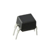
IRFD120PBF
Vishay Siliconix
MOSFET N-CH 100V 1.3A 4DIP
1808AA560JAT1A
KYOCERA AVX
CAP CER 56PF 1KV NP0 1808
MIC2954-08YM
Microchip Technology
IC REG LIN POS ADJ 250MA 8SOIC
CL05A105KA5NNNC
Samsung Electro-Mechanics
CAP CER 1UF 25V X5R 0402
G3VM-61D
Omron Electronics Inc-EMC Div
SSR RELAY SPST-NO 500MA 0-60V
A10192H
Antenova
A10192H FUSCA 2.4GHZ SMD HALOGEN
TSM160N10LCR RLG
Taiwan Semiconductor Corporation
MOSFET N-CH 100V 46A 8PDFN
SPD04N60C2
Infineon Technologies
N-CHANNEL POWER MOSFET
EPM7160EQI160-15
Altera
IC CPLD 160MC 15NS 160QFP
LMH6504MM
Texas Instruments
IC VARIABLE GAIN 1 CIRC 8VSSOP
BCM847BS-7
Diodes Incorporated
GENERAL PURPOSE TRANSISTOR SOT36
BA033F
Rohm Semiconductor
IC REG LINEAR 3.3V 1A TO252 -

EL5462ISZ
Renesas Electronics America Inc
IC OPAMP CFA 4 CIRCUIT 14SOIC
HA5013IP
Harris Corporation
HA5013 - TRIPLE, 125MHZ VIDEO AM
EPM240GT100C5
Altera
IC CPLD 192MC 4.7NS 100TQFP
OBS025ZH
Bel Power Solutions
DC DC CONVERTER 12V 25W
HIP6304CB
Intersil
SWITCHING CONTROLLER
MAX14662ETI+
Analog Devices Inc./Maxim Integrated
IC SWITCH SPST-NOX8 1OHM 28TQFN
04023U1R5CAT2A
KYOCERA AVX
CAP CER 1.5PF 25V NP0 0402
HCPL-2730
Broadcom Limited
OPTOISO 3.75KV 2CH DARLNG 8-DIP
RT0805BRE07120RL
YAGEO
RES SMD 120 OHM 0.1% 1/8W 0805
NJU7741F15-TE1
Nisshinbo Micro Devices Inc.
IC REG LINEAR 1.5V 100MA SOT23-5
CSTCE20M0V13C99-R0
Murata Electronics
CERAMIC RES 20.0000MHZ 15PF SMD
5V41234NLG
Renesas Electronics America Inc
IC CLK GEN SPRED SPECTRM 16VFQFP
LTC2366ITS8#TRPBF
Analog Devices Inc.
IC ADC 12BIT SAR TSOT23-8
MAC15A8G
onsemi
4 QUADRANT LOGIC LEVEL TRIAC, 60
KSC1730YTA
Fairchild Semiconductor
RF SMALL SIGNAL TRANSISTOR
TMK212SD153KD-T
Taiyo Yuden
CAP CER 0.015UF 25V 0805
NCV553SQ15T1G
onsemi
IC REG LINEAR 1.5V 80MA SC82AB
MIC38C44-1YN
Microchip Technology
IC OFFLINE SWITCH MULT TOP 14DIP -

MCP111-300E/TO
Microchip Technology
IC SUPERVISOR 1 CHANNEL TO92-3
SN65C1168EPWR
Texas Instruments
IC TRANSCEIVER FULL 2/2 16TSSOP
GALI-33+
Mini-Circuits
IC AMP CELLULAR 0HZ-4GHZ SOT89
XC17S50APD8C
AMD
IC PROM SER 50000 C-TEMP 8-DIP
EM6353BZ2SP3B-4.6+
EM Microelectronic
ULTRA LOW POWER RESET CIRCUIT WI
AR0132AT6M00XPEA0-DRBR
onsemi
IMAGE SENSOR RGB CMOS
MAX1951ESA+
Analog Devices Inc./Maxim Integrated
IC REG BUCK ADJUSTABLE 2A 8SOIC
GRM21BR71C335KA73L
Murata Electronics
CAP CER 3.3UF 16V X7R 0805
CL32A226KAJNFNE
Samsung Electro-Mechanics
CAP CER 22UF 25V X5R 1210
MMA02040C9092FB000
Vishay Beyschlag/Draloric/BC Components
RES 90.9K OHM 1% 2/5W MELF 0204
NDS356P
Fairchild Semiconductor
MOSFET P-CH 20V 1.1A SUPERSOT3
CPC7594BATR
IXYS Integrated Circuits Division
IC TELECOM INTERFACE 16SOIC
SC4810BITSTRT
Semtech Corporation
IC REG CTRLR FWRD CONV 16TSSOP
C1005X8R2A151K050BE
TDK Corporation
CAP CER 150PF 100V X8R 0402
SMCJ43CA-13-F
Diodes Incorporated
TVS DIODE 43VWM 69.4VC SMC
LC5512MB-75F256C
Lattice Semiconductor Corporation
IC CPLD 512MC 7.5NS 256FPBGA
TL072IDT
STMicroelectronics
IC OPAMP JFET 2 CIRCUIT 8SOIC
MCP1703AT-2502E/CB
Microchip Technology
IC REG LIN 2.5V 250MA SOT23A-3