Mastering SR Latches: Symbols, Functions, and Practical Applications
An SR latch is an asynchronous circuit that operates independently of clock signals, making it a versatile tool in various applications. It maintains a binary state—either high (1) or low (0)—and can store a single bit of information, which it holds until new input signals dictate a change. This basic binary storage element is constructed using two cross-coupled logic gates, typically NOR or NAND gates. The set input (S) activates the latch, setting the output (Q) to high, while the reset input (R) sets the output to low. However, simultaneous high signals on both inputs lead to an undefined state, a condition designers must avoid. SR latches are not just theoretical constructs; they are implemented in practical systems to hold temporary data, support intermediate processing results, and even manage error detection in critical applications such as aerospace and medical devices, showcasing their indispensability in digital circuit design.Catalog
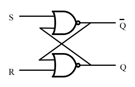
Figure 1: SR Latch
What is an SR Latch?
An SR latch, or Set-Reset latch, is a basic binary storage element that belongs to the category of asynchronous circuits. Unlike synchronous circuits, SR latches operate without a clock signal, relying solely on the direct control of input signals. This allows them to function independently within digital circuits. An SR latch can maintain two stable states: high (1) and low (0), enabling it to store a single bit of information until updated by new input signals.
Constructing an SR latch typically involves two cross-coupled logic gates, commonly NOR gates or NAND gates. In an SR latch design using NOR gates, the output of each gate is connected to the input of the other, forming a feedback loop. This configuration ensures that the latch can swiftly change states based on the input signals while maintaining stability until a new input prompts a change.
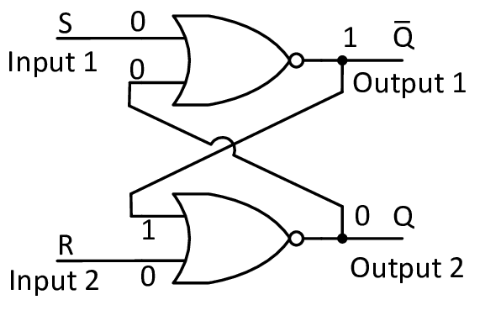
Figure 2: SR Latch (2)
Set Input (S): When the set input (S) is activated (high), the latch output (Q) switches to high (1).
Reset Input (R): When the reset input (R) is activated (high), the output (Q) switches to low (0).
Both Inputs High: If both S and R inputs are high simultaneously, the latch enters an undefined state, which should be avoided in design.
SR latches are essential for temporary data storage and intermediate result holding in digital systems. They are the foundational elements in more complex sequential circuits like multi-bit shift registers, memory units, and certain types of counters.
In these applications, SR latches provide stable data retention and can quickly respond to changes in external signals, ensuring the efficient operation of the entire electronic system.
Another critical application of SR latches is in error detection and correction logic within digital circuits. Due to their ability to hold a stable state, they can monitor system status changes and quickly revert to a predefined safe state upon detecting an anomaly. This feature is particularly valuable in high-reliability systems such as aerospace and medical devices.
Symbol of the SR Latch
Understanding its symbol and structure is fundamental to grasping its operation and practical use. In circuit diagrams, the SR latch typically has two main input ports labeled S (Set) and R (Reset). These inputs control the latch's output state, commonly represented as Q. Some designs also feature the inverse output, labeled Q', which provides the opposite state of Q.
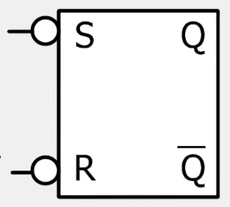
Figure 3: Symbol of the SR Latch
An SR latch is often represented by a rectangular symbol with inputs S and R and an output Q. In some cases, the output Q' is also shown. This clear labeling allows circuit designers to quickly identify the component's function and its role within the larger circuit.
A common variant of the SR latch includes a clock (CLK) input. The CLK input ensures that state changes occur in sync with the clock signal, enabling precise timing control. In this setup, even if S or R is activated, the latch's state only updates when the CLK signal meets specific conditions, usually on the rising or falling edge. This prevents errors caused by input signal glitches or unintended changes.
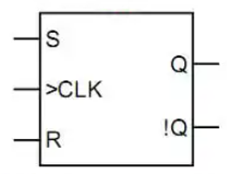
Figure 4: Symbol of the Clock-Gated SR Latch
The clocked SR latch symbol includes the S, R, and CLK inputs inside a rectangle. This standardized representation helps designers understand the latch's functionality and its timing requirements. For example, in high-performance computing or complex data transfer systems, careful CLK control ensures data is stored and transferred accurately at each processing stage, optimizing overall system performance and reliability.
Precise control of SR latch inputs is important, particularly in designing high-speed and large-capacity memory or temporary data buffers. By designing logic circuits to manage S and R activation, complex functions such as data loading, clearing, or state resetting can be achieved. Accurate CLK signal control ensures that all data operations follow a predefined timing sequence, significantly enhancing system efficiency and data processing capability.
A deep understanding of the SR latch's symbol and structure aids not only in correct circuit design and troubleshooting but also in executing complex digital logic operations and improving system performance. This is especially critical in applications requiring high reliability and precise control, such as aerospace and medical devices.
Types of Latches and Their Working Principles
Latches are fundamental components in electronic design, offering diverse functions and wide applications. The main types of latches are SR latches and D latches, each with unique operations and use cases.
SR Latch
The SR latch, or Set-Reset latch, is a basic storage device controlled by its two inputs, S (Set) and R (Reset).
When the S input receives a high signal, the output Q becomes high, indicating the data is set. When the R input receives a high signal, the output Q becomes low, indicating the data is reset. If both S and R inputs are high simultaneously, the latch enters an undefined state, causing potential output instability. This condition must be avoided in design. The SR latch's direct response to input signals makes it useful in situations requiring quick reaction.
D Latch
The D latch, also known as a Data latch or Transparent latch, offers more complex control with data input D and clock signal CLK.
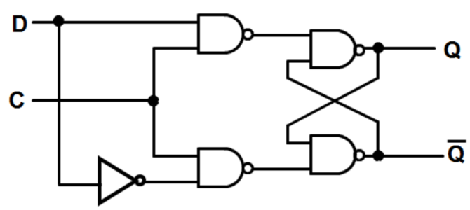
Figure 5: D Latch
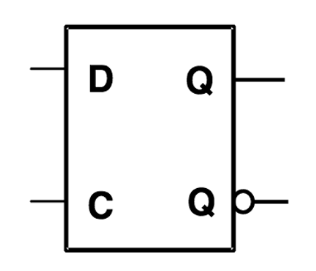
Figure 6: D Latch Symbol
When CLK is high, the output Q follows the input D, allowing data to pass through the latch freely. When CLK goes low, the current value of D is locked, and the output Q remains constant until the next CLK high signal. This mechanism makes the D latch ideal for temporarily storing data to synchronize different processing speeds within a system.
SR and D latches have an unparalleled role in data storage and state machine logic. Due to their direct input level response, latches are essential in designing asynchronous circuits. They provide vital functions for complex data transfers and power management systems, effectively storing state information to ensure stable operation. Proper use of these latches can significantly improve circuit reliability and efficiency, making them indispensable in modern electronic systems.
Truth Table of an SR Latch
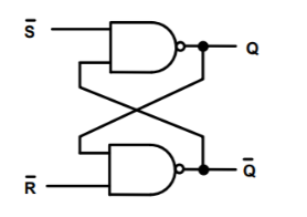
Figure 7: SR NAND Latch
|
S |
R |
Q |
Q' |
Note |
|
0 |
0 |
1 |
1 |
FORBIDDEN |
|
0 |
1 |
1 |
0 |
SET |
|
1 |
0 |
0 |
1 |
RESET |
|
1 |
1 |
Q |
Q' |
RETAIN |
Chart 1: Truth Table of SR Latch Using NAND Gates
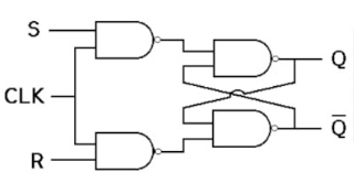
Figure 8: SR NOR Latch
|
S |
R |
Q |
Q' |
Note |
|
0 |
0 |
Q |
Q' |
RETAIN |
|
0 |
1 |
1 |
0 |
RESET |
|
1 |
0 |
0 |
1 |
SET |
|
1 |
1 |
0 |
0 |
FORBIDDEN |
Chart 2: Truth Table of SR Latch Using NOR Gates
Now we take the truth table of the SR latch using NOR gate as an example to understand the meaning of the truth table of the SR latch.
Input and Output States
Both S and R are 0: The latch remains in its current state. The output Q stays the same, whether it is 0 or 1.
S is 0 and R is 1: The latch resets, forcing the output Q to 0.
S is 1 and R is 0: The latch sets, making the output Q equal to 1.
Both S and R are 1: This condition is invalid or undefined, often referred to as the "forbidden" state in an SR latch. In this case, Q and Q' both equal 0, leading to an ambiguous output.
When S and R are both 0, the latch does nothing and simply holds its current value. This is useful for maintaining the state without changes.
When S is 0 and R is 1, the latch is explicitly told to reset, making sure Q is 0 regardless of its previous state. This is a straightforward way to clear the latch.
When S is 1 and R is 0, the latch is set, ensuring Q becomes 1. This is how you store a '1' in the latch.
When S and R are both 1, the state is not allowed because it causes both outputs to be 0, which is contradictory and unreliable. Designers must avoid this condition to ensure stable operation.
Advantages and Disadvantages of Latches
Latches are widely used in digital circuit design due to their simplicity and low cost. These characteristics enable latches to operate at high speeds with low power consumption, making them ideal for high-speed digital systems. For instance, in processor register files, latches can quickly store and retrieve data, significantly boosting processing speed and efficiency.
Advantages of Latches
Simplicity and Cost-Effectiveness: Latches are straightforward components that are inexpensive to implement in digital circuits.
High Speed and Low Power: Their design allows for fast operation with minimal power consumption, which is critical in high-speed digital systems.
Efficiency in Data Handling: In applications like processor register files, latches provide quick data storage and retrieval, enhancing overall system performance.
Disadvantages of Latches
Despite their advantages, latches have notable limitations in certain designs and applications.
Unpredictable Behavior in Asynchronous Designs: Without clock signal control, latches can behave unpredictably. In SR latches, if both Set (S) and Reset (R) inputs are high simultaneously, the output becomes undefined, leading to instability. This is problematic in real-time control or safety-critical applications, where reliable output is crucial.
Complex Timing Design: Designing with latches requires careful timing considerations. Engineers must account for signal propagation delays and race conditions to avoid timing errors. Improper design can result in data changes before the clock signal stabilizes, causing data corruption or incorrect data capture. This necessitates a deep understanding of timing analysis and circuit behavior.
To address these challenges, specific design techniques and strategies can be employed:
Synchronization Mechanisms: Adding synchronization mechanisms can help manage asynchronous inputs and mitigate unpredictable behavior.
Custom Clock Management: Implementing customized clock management strategies can ensure that data is latched correctly and at the right times.
Use of EDA Tools: Modern Electronic Design Automation (EDA) tools offer advanced analysis and optimization capabilities. These tools help predict and resolve timing and synchronization issues during the design phase, improving the reliability and performance of digital systems using latches. They assist designers in identifying potential problems early, ensuring the final product operates reliably under various conditions.
Practical Applications of SR Latches
SR latches, known for their ability to quickly and reliably maintain state, are widely used in various electronic systems. They excel in scenarios requiring temporary data storage or state retention.
Temporary Data Storage
SR latches are often used in cache memory to temporarily store data. This allows the system to quickly access frequently used data, significantly boosting the data processing capabilities and efficiency of large-scale processors.
Storage Register Files
In processors, SR latches enable rapid storage and retrieval of data in register files, enhancing processing speed and overall system performance.
Maintaining Control Signals
In digital control systems, SR latches are useful in maintaining the state of certain control signals until external conditions or system logic dictates a change. Also, they help in retaining states within the system, ensuring consistent performance in operations that require precision and reliability.
Trigger and Counter Circuits
SR latch-based flip-flops are commonly used in circuits requiring synchronized operation, such as digital clocks and timers. They control count pulses, ensuring accurate timekeeping and reliable performance. These circuits rely on SR latches to maintain accurate counts, which facilitates timing and sequencing in digital systems.
Mechanical Interactions
SR latches are effective in eliminating mechanical bounce in switches. A mechanical bounce occurs when a switch generates rapid, repetitive signal changes due to poor contact. SR latches stabilize the output signal, preventing errors caused by noisy signals.
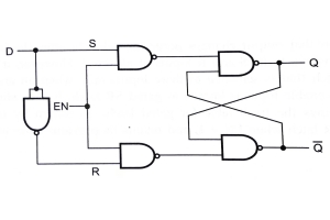
SR Flip-Flop
An SR flip-flop, often called an edge-triggered Set-Reset flip-flop, consists of two interconnected SR latches. This dual-latch structure allows it to respond to specific clock signal edges (either rising or falling) to change its state. This is achieved through special logic control between the latches. The output of the first latch becomes part of the input for the second latch, and the output of the second latch, in turn, influences the first latch, creating an interlocking feedback loop.
Figure 7: SR Flip-Flop
The SR flip-flop changes state precisely at the clock signal's rising or falling edge. The interlocking feedback between the two SR latches ensures that the flip-flop only changes state in response to the clock edge, providing stable and reliable output.
In microprocessors and digital signal processors, SR flip-flops are used for data sampling and storage. They capture and stabilize data at specified clock edges, ensuring reliable subsequent data processing and analysis.
The edge-triggering mechanism helps avoid race conditions, where different parts of the circuit may change state at the same time without synchronization, potentially resulting in unstable or incorrect outputs. SR flip-flops are crucial in implementing specific communication protocol logic, such as frame synchronization and error detection. Their stability and fast response time help maintain data transmission quality and system reliability.
Forbidden States in SR Latches and SR Flip-Flops
When designing SR latches and SR flip-flops using NAND and NOR gates, we all need to pay attention to managing and avoiding inhibited states. A forbidden state occurs when both the Set (S) and Reset (R) inputs are simultaneously high (for NAND gates) or low (for NOR gates). This combination leads to an indeterminate output state, as the output depends on the previous state of the circuit, making it unpredictable.
Forbidden States in NAND Gate SR Latches
When both S and R are low, both outputs go high, which violates the latch's complementary output characteristic. This results in an indeterminate state.
Forbidden States in NOR Gate SR Latches
When both S and R are high, both outputs go low, also creating an indeterminate state. This can lead to unpredictable behavior in the circuit.
Practical Approaches to Avoid Forbidden States
Adding Control Logic
Use additional logic gates to monitor the states of S and R. If both inputs trend towards a forbidden state, automatically adjust one input to prevent the indeterminate state. This ensures that the outputs remain stable and predictable. Implement a logic gate that intervenes when S and R are both high (or low), adjusting one input to maintain a valid state.
Software Simulation and Hardware Testing
Conduct thorough software simulations to identify potential forbidden states under various operating conditions. This allows designers to spot and correct logical errors before physical implementation. Perform extensive hardware testing to validate that the circuit handles all input combinations correctly. This step helps to ensure that the latch or flip-flop operates reliably in real-world scenarios.
Conclusion
The versatility and reliability of SR latches underscore their significance in digital circuit design. By exploring the nuanced behavior of SR latches through their symbol representations, truth tables, and practical applications, we gain a comprehensive understanding of their operation and importance. Despite the potential pitfalls of undefined states in asynchronous designs, strategic implementation of control logic and extensive simulation can mitigate these risks. Advanced Electronic Design Automation (EDA) tools further enhance the reliability and performance of circuits incorporating SR latches by predicting and resolving timing and synchronization issues. Whether used in temporary data storage, control signal maintenance, or error detection, SR latches prove to be foundational in creating robust and efficient digital systems. Their role in high-speed memory operations and synchronous data processing in complex applications exemplifies their enduring relevance. As technology advances, the principles governing SR latches continue to inform and inspire innovations in digital electronics, ensuring that these elementary components remain integral to the development of sophisticated and reliable electronic devices.
Frequently Asked Questions [FAQ]
1. What is an SR latch?
An SR latch, or Set-Reset latch, is a fundamental binary storage element used in digital circuits. It is an asynchronous circuit, meaning it operates without a clock signal, relying on the direct control of its inputs to change states.
2. What is the function of SR in logic?
In logic, the SR (Set-Reset) inputs control the state of the latch.
3. What type of logic gate does an SR latch use?
An SR latch typically uses either NOR gates or NAND gates. In a NOR gate-based SR latch, the output of each NOR gate is fed back into the input of the other, creating a stable feedback loop. In a NAND gate-based SR latch, a similar feedback configuration is used, but the logic levels are inverted compared to the NOR gate-based latch. Both configurations achieve the same basic functionality of maintaining a binary state based on the Set and Reset inputs.
4. How does a latch work?
A latch works by using feedback to maintain its output state based on the inputs provided. In an SR latch, the Set (S) and Reset (R) inputs control the state of the output (Q). When the Set input is activated (high), the output is set to high (1). When the Reset input is activated (high), the output is reset to low (0). The feedback loop in the latch's design ensures that once an output state is established, it remains stable until a new input signal changes it.
5. What is the disadvantage with an SR latch?
The primary disadvantage of an SR latch is the undefined state that occurs when both Set (S) and Reset (R) inputs are high simultaneously. This condition leads to an indeterminate output state, which can cause instability and unpredictable behavior in digital circuits. This "forbidden" state must be avoided in design to ensure reliable operation.
SR latch, Set-Reset latch, asynchronous circuit, binary storage element, digital circuits, NOR gates, NAND gates, feedback loop, high state, low state, undefined state, clock signal, direct control, temporary data storage, intermediate result holding, error detection, aerospace applications, medical devices, circuit design, clocked SR latch, input signals, symbol and structure, high-speed memory, data buffers, timing control, precise control, state retention, microprocessors, digital signal processors, data sampling, data storage, edge-triggered, SR flip-flop, interlocking feedback, race conditions, communication protocol logic, frame synchronization, error detection, signal glitches, Electronic Design Automation, EDA tools, synchronization mechanisms, custom clock management, timing errors, propagation delays, race conditions, complex data transfers, power management systems, mechanical bounce, practical applications, digital control systems, logic gates, software simulations, hardware testing, forbidden states, latch reliability.
About us
ALLELCO LIMITED
Read more
Quick inquiry
Please send an inquiry, we will respond immediately.
A guide to the basics of D flip-flops - circuits, truth tables, types, advantages and limitations
on May 17th
Comparative Guide to Analyzing rheostat and Potentiometers
on May 17th
Popular Posts
-
What is GND in the circuit?
on January 1th 2937
-
RJ-45 Connector Guide: RJ-45 Connector Color Codes, Wiring Schemes, R-J45 Applications, RJ-45 Datasheets
on January 1th 2498
-

Fiber Connector Types: SC Vs LC And LC Vs MTP
on January 1th 2089
-
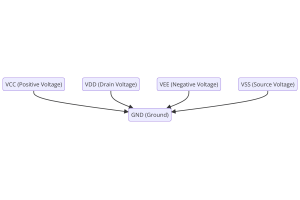
Understanding Power Supply Voltages in Electronics VCC, VDD, VEE, VSS, and GND
on November 9th 1888
-

Comparison Between DB9 and RS232
on January 1th 1759
-

What Is An LR44 Battery?
Electricity, that ubiquitous force, quietly permeates every aspect of our daily lives, from trivial gadgets to life-threatening medical equipment, it plays a silent role. However, truly grasping this energy, especially how to store and efficiently output it, is no easy task. It is against this background that this article will focus on a type of coin cell battery that may seem insignificant on the...on January 1th 1712
-
Understanding the Fundamentals:Inductance Resistance, andCapacitance
In the intricate dance of electrical engineering, a trio of fundamental elements takes center stage: inductance, resistance, and capacitance. Each bears unique traits that dictate the dynamic rhythms of electronic circuits. Here, we embark on a journey to decipher the complexities of these components, to uncover their distinct roles and practical uses within the vast electrical orchestra. Inductan...on January 1th 1651
-

CR2430 Battery Comprehensive Guide: Specifications, Applications and Comparison to CR2032 Batteries
What is CR2430 battery ?Benefits of CR2430 BatteriesNormCR2430 Battery ApplicationsCR2430 EquivalentCR2430 VS CR2032Battery CR2430 SizeWhat to look for when buying the CR2430 and equivalentsData Sheet PDFFrequently Asked Questions Batteries are the heart of small electronic devices. Among the many types available, coin cells play a crucial role, commonly found in calculators, remote controls, and ...on January 1th 1548
-
What Is RF and Why Do We Use It?
Radio Frequency (RF) technology is a key part of modern wireless communication, enabling data transmission over long distances without physical connections. This article delves into the basics of RF, explaining how electromagnetic radiation (EMR) makes RF communication possible. We will explore the principles of EMR, the creation and control of RF signals, and their wide-ranging uses. The article ...on January 1th 1537
-

CR2450 vs CR2032: Can The Battery Be Used Instead?
Lithium manganese batteries do have some similarities with other lithium batteries. High energy density and long service life are the characteristics they have in common. This kind of battery has won the trust and favor of many consumers because of its unique safety. Expensive tech gadgets? Small appliances in our homes? Look around and you'll see them everywhere. Among these many lithium-manganes...on January 1th 1505
HOT Part Number
-
SKY65405-21
Skyworks Solutions Inc.
IC AMP 802.11B/G/N 2.4GHZ 6DFN
VLF10040T-1R0N9R7
TDK Corporation
FIXED IND 1UH 9.7A 5.2 MOHM SMD
SZ1SMA13CAT3G
Littelfuse Inc.
TVS DIODE 13VWM 21.5VC SMA
PI3B16244AE
Diodes Incorporated
IC BUS SWITCH 4 X 1:1 48TSSOP
DB3J315E0L
Panasonic Electronic Components
DIODE ARRAY SCHOTTKY 30V SMINI3
LTM9002IV-LA#PBF
Analog Devices Inc.
IC RCVR IF/BASEBAND 14B 108LGA
L4984D
STMicroelectronics
IC PFC CTRLR CCM 10SSOP
1812L035/60MR
Littelfuse Inc.
PTC RESET FUSE 60V 350MA 1812
ADP3309ART-3.3-RL7
Analog Devices Inc.
IC REG LINEAR 3.3V 100MA SOT23-5
NLCV32T-R33M-PFR
TDK Corporation
FIXED IND 330NH 2.1A 42 MOHM SMD
IRF7805ZTRPBF
Infineon Technologies
MOSFET N-CH 30V 16A 8SO
UCC27322MDEP
Texas Instruments
IC POWER MANAGEMENT
TPA2038D1YFFR
Texas Instruments
IC AMP CLASS D MONO 3.24W 9DSBGA
TLE2425MDR
Texas Instruments
IC VREF GND REF 0.8% 8SOIC
SMF20CA
Littelfuse Inc.
TVS DIODE 20VWM 32.4VC SOD123F
600F180JT250XT
American Technical Ceramics
CAP CER 18PF 250V C0G/NP0 0805
SG1626J
Microchip Technology
HALF BRIDGE DRIVER, INVERTING, H
MAX4051ACSE
Analog Devices Inc./Maxim Integrated
IC MUX 8:1 100OHM 16SOIC -

AT97SC3203-X9M10
Atmel
AVR RISC MCU
AD7507JQ
Analog Devices Inc.
IC SWITCH SP4T X 2 28CDIP
VE-2N1-EV
Vicor Corporation
DC DC CONVERTER 12V 150W
ISL3178EIUZ-T
Renesas Electronics America Inc
IC TRANSCEIVER HALF 1/1 8MSOP
P6SMB47A
Meritek
TVS DIODE 40.2VWM 64.8VC
87758-4216
Molex
2MM MGRID VHDR 38AULF 42CKT
AZ1117EH-1.8TRG1
Diodes Incorporated
IC REG LINEAR 1.8V 1A SOT223
ATF-511P8-TR1
Broadcom Limited
FET RF 7V 2GHZ 8-LPCC
V110B36H200BG2
Vicor Corporation
DC DC CONVERTER 36V 200W
SN74HC174PWR
Texas Instruments
IC FF D-TYPE SNGL 6BIT 16TSSOP
JS28F128P30B85A
Numonyx
IC FLASH 128MBIT PARALLEL 56TSOP
TPS22924CYZPRB
Texas Instruments
IC PWR SWITCH N-CHAN 1:1 6DSBGA
CSD17311Q5
Texas Instruments
MOSFET N-CH 30V 32A/100A 8VSON
51786-003LF
Amphenol ICC (FCI)
CONN HDR BLADE PWR 30POS EDGE MT
XC2C512-10FTG256I
AMD
IC CPLD 512MC 9.2NS 256FTBGA
CL10B153JB8NNNC
Samsung Electro-Mechanics
CAP CER 0.015UF 50V X7R 0603
VI-BTL-EV
Vicor Corporation
DC DC CONVERTER 28V 150W
ZMM5252B
Rectron USA
DIO ZENER GLASS 24V 500MW LL-34 -
EMK212BJ106KG-T
Taiyo Yuden
CAP CER 10UF 16V X5R 0805
LT3507AHFE#TRPBF
Linear Technology
LT3507A - TRIPLE MONOLITHIC STEP
HUF75639S3S
onsemi
MOSFET N-CH 100V 56A D2PAK
TLV2375IPWRG4
Texas Instruments
IC OPAMP GP 4 CIRCUIT 16TSSOP
C2012C0G1H103J060AA
TDK Corporation
CAP CER 10000PF 50V C0G 0805
STP85N3LH5
STMicroelectronics
MOSFET N-CH 30V 80A TO220AB
EVK105RH1R3BW-F
Taiyo Yuden
CAP CER 1.3PF 16V R2H 0402
PGA281AIPW
Texas Instruments
IC OPAMP PGA 1 CIRCUIT 16TSSOP
74AC257SCX
onsemi
IC MULTIPLEXER 4 X 2:1 16SOIC
SS441R
Honeywell Sensing and Productivity Solutions
MAGNETIC SWITCH UNIPOLAR TO92-3
V30M120M-E3/4W
Vishay General Semiconductor - Diodes Division
DIODE SCHOTTKY 15A 120V TO-220AB
IR2233S
Infineon Technologies
IC GATE DRVR HALF-BRIDGE 28SOIC
TLC27L4CPWR
Texas Instruments
IC CMOS 4 CIRCUIT 14TSSOP
SN74172N
Texas Instruments
MULTI-PORT SRAM, 8X2, 50NS
DP83901AV
Texas Instruments
IC CONTROLLR SER NETWK IN 68PLCC
ISL60002CIH325
Renesas Electronics America Inc
IC VREF SERIES 0.1% SOT23-3
RFP15N08L
Harris Corporation
N-CHANNEL POWER MOSFET
SN74AHC32QPWRG4Q1
Texas Instruments
IC GATE OR 4CH 2-INP 14TSSOP