on January 17th
707
Guidelines for the use of leaded and lead-free solder
In the intricate landscape of modern electronic manufacturing, the choice of welding technology and solder is not just a technicality. It's a decision that deeply influences product performance, reliability, and environmental adaptability. Central to this is the solder – the core medium that fuses electronic components to circuit boards. The physical properties, chemical composition and environmental compatibility of solder play a decisive role in determining the quality and service life of electronic devices.
Delving into the nuances of circuit board solders, this article highlights the contrasts and practical implications of lead and lead-free variants. We'll journey from the microscopic analysis of solder composition to the broader aspects of manufacturing processes and environmental impacts, painting a comprehensive picture of soldering technology's evolution and future trends.
Solder is no mere metal alloy. It's a critical medium in electronic manufacturing, binding components to boards. Typically comprising tin, lead, copper, silver, and other elements in specific ratios, solder's low melting points facilitate easy melting and re-solidification, ensuring good electrical conductivity and mechanical stability.
In manufacturing printed circuit boards (PCBs), mastery in soldering is often synonymous with product quality. The soldering process, intricate and demanding, involves heating a solder alloy beyond its melting point and applying it precisely between the electronic component's pins or leads and the PCB's copper traces. This process requires not only precise temperature control to avoid circuit damage due to overheating but also a careful balance of soldering time and volume to achieve strong mechanical and electrical connections.
Upon cooling, the solder crystallizes into what's known as a solder joint. These connectors can extend the service life of the equipment and must have sufficient mechanical strength and long-lasting electrical conductivity. High-quality joints are characterized by a smooth surface, absence of bubbles or cracks, a proper wetting angle, and robust metal contact with pads and leads. The solder's composition, the welding technique, and the cooling process are all vital to these joints' integrity.
Environmental considerations and health concerns have spurred the shift to lead-free solders. While traditional solder often includes lead, the trend in modern electronics manufacturing leans increasingly towards lead-free alternatives. These substitutes, mainly tin-based and supplemented with silver, copper, or other metals, mirror the melting points and properties of traditional solders while aligning with environmental standards.
The ramifications of solder selection and soldering techniques on the overall quality and dependability of electronic manufacturing are profound. As demands for performance, reliability, and environmental stewardship escalate in the electronics industry, so too do innovations in solder technology and welding processes.
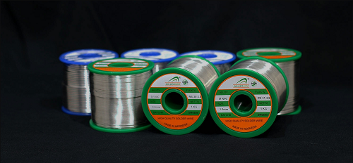
In the multifaceted world of electronics manufacturing, a myriad of solder types exists, each boasting its own set of unique applications and characteristics. Core among them are solder wire and solder paste, which are widely used in different soldering environments and methods.
Solder wire, a slender alloy wire, is extensively utilized in manual soldering. Typically a blend of tin and lead, it's available in lead-free variants too. Its diameter varies, allowing for selection based on the welding object's fineness. It works in tandem with a soldering iron, adept at precisely connecting electronic components to the PCB. Especially favored in prototyping, repair, or small-scale production, its versatility shines across diverse welding demands.
Then, there's solder paste – a concoction of minuscule solder particles and flux. It takes center stage in surface mount technology (SMT), tailored for large-scale, automated production. In SMT, this paste is meticulously applied to precise PCB areas using stencils or dispensers. Electronic components are placed atop these paste-coated zones. The board then enters a reflow oven; a heating sequence ensues, melting the tiny solder particles to forge strong electrical bonds.
The solder paste's composition and quality are paramount in SMT. Ideal solder paste should exhibit excellent printability, sufficient tack to secure components, superior wetting for robust joint formation, and strong oxidation resistance to avert joint degradation. Its formulation also must consider the soldering process's thermal cycling and compatibility with PCB and component materials.
Thus, solder wire and solder paste stand as the two pillars in electronics manufacturing solder types. Selecting between them hinges not only on the process's automation level and throughput but also on cost, quality control, and environmental considerations. As demands for precision and reliability in the electronics industry soar, so too does the drive for innovation and enhancement in solder technologies.
In the practical application of circuit board soldering, the decision between lead solder and lead-free solder depends on the balance between technical strength and environmental considerations. Each type of solder has its physical properties, specific applications, and environmental effects.
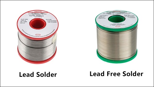
Lead solder, typically a blend of tin (Sn) and lead (Pb) in proportions like the common Sn63Pb37 alloy with a 183°C melting point, offers certain advantages. Its lower melting point allows soldering at reduced temperatures, minimizing thermal stress on circuit boards and delicate electronic components. This reduction in thermal stress diminishes the likelihood of sheet bending and layer separation, thus bolstering the overall reliability of electronic devices. Moreover, lead solder's superior wetting properties yield smoother, brighter solder joints, simplifying inspection and repair tasks.
However, the landscape shifts when considering international regulations such as the Waste Electrical and Electronic Equipment Directive (WEEE) and the Restriction of Hazardous Substances Directive (RoHS). These have curtailed or forbidden lead usage in specific scenarios, citing its toxicity and long-term environmental risks. Consequently, the industry pivots towards lead-free solder. Predominantly comprising tin (Sn), copper (Cu), silver (Ag), nickel (Ni), and zinc (Zn), tin-copper alloys like Sn99.3Cu0.7 are prevalent. Lead-free solders typically have higher melting points, often exceeding 217°C, necessitating increased soldering temperatures and potentially elevating thermal stress on circuit boards.
Lead-free solder, while environmentally safer, trails behind in wettability compared to its lead-based counterpart. This disparity can affect solder joint smoothness. To enhance wettability and combat oxidation, a greater reliance on flux is often necessary. Additional challenges with lead-free solder include the complexities of visually inspecting solder joints and concerns regarding long-term joint reliability.
The selection between lead and lead-free solder isn't just driven by the welding process or product application but also by environmental regulations and market demands. As lead-free solder technology evolves, its performance is steadily improving. Nevertheless, in high-reliability applications, lead solder maintains its relevance. The electronics manufacturing industry must continue to evolve its welding technologies, striving to align with stringent environmental standards without compromising product performance and reliability.
4.1 Lead-free solder
Melting point: It typically exceeds 217°C, hovering 20°C to 40°C above the lead variant. Consequently, soldering necessitates higher peak reflow temperatures, often ranging from 245°C to 260°C. Such temperatures might surpass the thermal endurance limits of certain electronic components, notably highly integrated ICs and precision elements. This necessitates a meticulous selection of lead-free solder, keeping in mind the thermal resistance of components.
Wetting properties: These are generally inferior to those of leaded solders. Issues like incomplete solder joints and solder bridging, or even hole formation, may arise. Combatting this involves precise temperature control, extended reflow durations, or the application of specific fluxes.
Heat aging resistance and reliability: In high-temperature settings, lead-free solder can prompt thermal aging, warping materials like resin and copper foil on circuit boards. Over time, this jeopardizes the board's physical and electrical integrity, undermining reliability.
Equipment requirements: Catering to the higher heating demands of lead-free solder, soldering equipment must ensure elevated temperature control accuracy and thermal stability. This might compel companies to invest in cutting-edge equipment or upgrade existing ones, thus inflating manufacturing costs.
Long-term durability and corrosion resistance: Lead-free solder trumps in resisting oxidation and corrosion. This bolsters the long-term stability of solder joints, particularly in harsh environments.
Cost-Effectiveness of the Manufacturing Process: Environmental regulations and technological advancements in lead-free solder are gradually reducing its cost.
4.2 Leaded solder
Melting point: Typically around 183°C. The lower melting point allows for reduced soldering temperatures, lessening the risk of damaging sensitive components.
Wetting performance: Its superior wetting performance ensures more uniform, complete solder joints, thus diminishing welding defects.
Environmental and Health Effects: Containing lead, a known health and environmental hazard, its usage, especially in consumer electronics, is increasingly limited by directives like RoHS (Restriction of Hazardous Substances Directive). Prolonged lead exposure can lead to neurological and other health issues.
Cost-Effectiveness of the Manufacturing Process: The lower melting point and excellent wettability of leaded solder offer cost and application benefits.
The choice between lead and lead-free solder hinges not just on their physical and chemical characteristics, but also on product application needs, manufacturing process nuances, environmental regulation constraints, and long-term health and environmental considerations. The electronics manufacturing industry faces the challenge of constantly refining welding processes and equipment, ensuring performance and reliability amidst tightening environmental standards.
Yet, leaded solder's use of toxic lead presents serious health and environmental concerns. The increasing awareness and regulation of lead's toxicity and bioaccumulation have led to a growing number of international environmental regulations, like the European Union’s Restriction of Hazardous Substances Directive (RoHS), restricting or banning lead-containing solders, especially in consumer electronics. This has driven the development of lead-free solder technology, which still seeks improvements in certain performance areas.
The decision between leaded and lead-free solders involves weighing advantages and disadvantages, considering the product's application requirements, the characteristics of the manufacturing process, and environmental regulations. The electronics manufacturing industry must persistently enhance lead-free solder technology, balancing product performance with stringent environmental standards. This choice of solder hinges not only on technical performance but also on health and environmental impacts. As understanding of the adverse effects of lead-containing solder grows, manufacturers increasingly opt for lead-free solder, aligning with tighter international environmental regulations and health considerations.
Lead-free solders, typically with a higher tin content, show better corrosion resistance, an advantage for PCBs in humid or corrosive environments like automotive electronics and outdoor communication equipment. This higher corrosion resistance prolongs product life, reduces repair costs, and maintains electrical connection reliability. However, lead-free solders generally have a broader melting point range, between 217°C and 227°C, higher than traditional lead-containing solders like Sn63Pb37. This necessitates higher soldering temperatures, risking more thermal damage to PCBs and sensitive components, such as circuit board warping, layer separation, and thermal expansion of copper wires. Transitioning to lead-free solder, therefore, requires a redesign of the soldering process, employing more heat-resistant materials and components.
The differences in corrosion resistance and melting points between lead-containing and lead-free solders crucially impact the design, manufacturing, and long-term performance of electronic products. Manufacturers must consider the application environment, performance requirements, cost-effectiveness, and health/environmental impact when selecting solder. As new materials and technologies evolve, more environmentally friendly and high-performing solder options are anticipated, meeting the electronics industry's growing needs for both sustainability and high performance.
Lead and lead-free solders each present unique characteristics and encounter different technical challenges and application limitations. These disparities profoundly impact product design, manufacturing processes, and the final product's reliability and eco-friendliness. Lead-based solder, renowned for its user-friendliness and lower melting point, remains a staple in many conventional electronics manufacturing scenarios. Its lower melting point, exemplified by the Sn63Pb37 alloy melting at 183°C, mitigates thermal stress on circuit boards and sensitive components, thereby diminishing the likelihood of heat-induced defects like warping and interlayer separation. Furthermore, lead solder's superior wettability ensures smoother, more even flow and robust, uniform solder joints.
However, with the surge in environmental consciousness and the enforcement of international regulations like the RoHS directive, the utilization of lead-containing solder has been stringently curtailed. These regulations aim to minimize the use of lead and other hazardous substances, safeguarding human health and the environment. Consequently, lead-free solder has become a necessity in regions adhering to these standards. Despite its clear environmental and health safety benefits, the technical challenges of lead-free solder are non-trivial. Its typically higher melting point, often exceeding 217°C, demands increased soldering temperatures, potentially exacerbating thermal stress on boards and components. Lead-free solder's inferior wettability might lead to inconsistent solder joint quality and compound the complexity of the soldering process. It is also susceptible to deposit formation, potentially impacting the reliability and aesthetics of solder joints.
Transitioning to lead-free solder, many manufacturers have had to revamp their soldering procedures, redesign circuit boards and components for higher soldering temperatures, and adopt advanced soldering techniques to counteract poor wetting and joint formation issues. While this transition necessitates additional investment in time and costs, it represents an unavoidable trend in the contemporary electronics industry, which prioritizes environmental, health, and safety considerations.
The selection between lead and lead-free solder in practical applications hinges on various factors, including product application requirements, manufacturing capabilities, and environmental and health considerations. With ongoing technological and material advancements, the efficacy of lead-free solders is anticipated to further improve, aligning with the electronics industry's escalating demands for high quality and environmental responsibility.
During the printed circuit board (PCB) manufacturing process, choosing the right solder plays a decisive role in ensuring soldering quality and the overall functionality of the PCB. Both lead and lead-free solders impart distinct influences across various soldering applications, affecting not only the soldering process but also the circuit board layout, component choice, and the performance of the end product.
Wave soldering, a prevalent technique for assembling through-hole components, involves passing the PCB through a wave of molten solder. This method capitalizes on capillary action and gravity for solder flow into vias and pads. Lead solder, known for its lower melting point, is advantageous in wave soldering, primarily as it mitigates thermal stress on the PCB. Moreover, its superior wetting properties facilitate the formation of smooth, uniform solder joints. However, environmental regulations have increasingly necessitated the adoption of lead-free solder in wave soldering. This alternative, with its higher melting point, demands more precise temperature control to avert PCB damage due to overheating.
Through-hole soldering, another widespread method, typically connects component pins to PCBs. Utilizing lead-free solder in this technique poses its own set of challenges, including the requisite for higher melting temperatures and reduced wettability. These issues can lead to incomplete solder joint formation, thereby elevating the likelihood of soldering defects. When employing lead-free solder, welding parameters such as temperature, time, and solder volume need meticulous control to ensure joint quality and reliability.
PCB manufacturers must weigh several factors in deciding between lead or lead-free solder. This decision encompasses considerations of the circuit board layout, the thermal sensitivity of selected components, and the application environment of the final product. For instance, designing dense or heat-sensitive circuit boards with lead-free solder may necessitate more intricate floor planning and thermal management strategies to mitigate the risks of thermal damage from higher soldering temperatures.

During complex welding jobs, especially in the electronics manufacturing industry, we deal with countless potential health risks and safety hazards. Safety prevention, therefore, must be placed at the forefront of our priorities. Achieving a safe welding process is no small feat. It necessitates a comprehensive array of preventive measures, including but not limited to personal protection, meticulous management of the work environment, and a thorough grasp of the materials and equipment involved.
The initial step in welding operations is the judicious selection of appropriate personal protective equipment (PPE). Personal protective equipment is more than just the basic three of safety goggles, heat-resistant gloves, and closed-footed shoes. It also encompasses specialized clothing to guard against welding sparks and, in scenarios necessitating it, a suitable respirator becomes indispensable. Respirators are crucial, particularly when the soldering process involves materials like lead-containing solder, notorious for emitting harmful fumes and gases.
During welding operations, particularly with the use of sizeable welding equipment, earplugs or earmuffs should be standard attire to shield against noise-induced damage. The safety management of the working environment is equally vital. At its core is ensuring optimal ventilation, which helps reduce the inhalation of toxic fumes and gases. Welding areas should be equipped with effective ventilation and exhaust systems, complemented by air purifiers. To mitigate the risk of fire caused by the accumulation of flammable materials, we first need to keep the work area dry and organized.
In terms of equipment use, we should strictly abide by operating procedures. This includes correct handling of soldering irons, encompassing heating, operation, and cooling procedures. The stability of the welding workpiece during operations is critical to prevent unintended contact with the heat source. Post-operation, ensuring that the soldering iron and other tools are safely turned off and allowed to cool sufficiently is key to avoiding burn injuries.
In any welding project, we need to first understand the materials and equipment and their potential risks. This knowledge is particularly important when dealing with lead-containing solder, which calls for additional safety measures. Understanding the composition of solder is fundamental. Also, being versed in the safe operation of various welding equipment and emergency response procedures is key to welding safety.
Safety measures in welding are not just a few steps; they form a complex, multi-tiered system. This system spans personal protection, diligent management of the work environment, strict adherence to equipment operation protocols, and deep material safety knowledge. By implementing these thorough measures, the potential health risks and safety hazards in welding operations can be greatly reduced.
A detailed analysis reveals that both leaded and lead-free solders play significant roles in electronic manufacturing. Leaded solder, favored for its excellent wetting properties and lower melting point, remains prevalent in numerous applications. However, environmental regulations increasingly restrict its use. Conversely, lead-free solder, despite initial technical challenges like a higher melting point and wettability issues, is continually evolving. Technological advancements are enhancing its performance, making it increasingly popular in the electronics industry.
Safety precautions in welding are an integral component of the manufacturing process. They encompass ensuring personal protection, maintaining safety in the work environment, and the safe handling of materials and equipment. The electronics manufacturing industry's growth is tethered not just to product performance and reliability. It also hinges on aligning with environmental protection trends. This alignment necessitates the continuous evolution and optimization of welding technologies and processes. This evolution benefits the growing need for environmental protection and human health.
Looking to the future, as new materials and technologies emerge, we anticipate the development of more environmentally friendly and higher-performing solder options. These advancements are expected to drive the electronics industry toward elevated levels of performance and sustainability.
Share: