Detailed Guide to Full Adder
Catalog
What is an Adder?
Half Adder
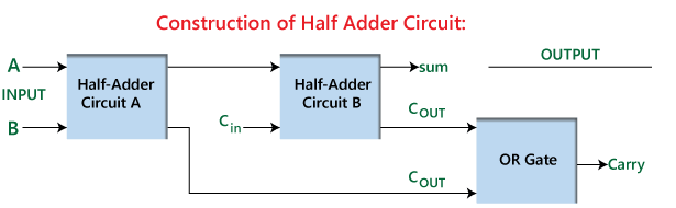
Full Adder
|
Parameters |
Half Adder |
Full Adder |
|
Description |
Half Adder is a combinational logic circuit that adds two 1-bit digits. The half-adder produces a sum of the two inputs. |
A full adder is a combinational logic circuit that performs an addition operation on three one-bit binary numbers. The full adder produces a sum of the three inputs and carry value. |
|
Previous carry |
The previous carry is not used. |
The previous carry is used. |
|
Inputs |
In Half adder, there are two input bits (A, B). |
In full adder, there are three input bits (A, B, Cin). |
|
Outputs |
The generated output is of two bits-Sum and Carry from the input of 2 bits. |
The generated output is of two bits-Sum and Carry from the input of 3 bits. |
|
Used as |
A half-adder circuit cannot be used in the same way as a full-adder circuit. |
A full adder circuit can be used in place of a half adder circuit. |
|
Feature |
It is simple and easy to implement |
The design of a full adder is not as simple as a half adder. |
|
Logical Expression |
Logical Expression for half adder is: S=a⊕b; C=a*b. |
Logical Expression for Full adder is: S=a⊕b⊕Cin; Cout=(a*b)+(Cin*(a⊕b)). |
|
Logic gates |
It consists of one EX-OR gate and one AND gate. |
It consists of two EX-OR, two AND gates, and one OR gate. |
|
Applications |
It is used in Calculators, computers, digital measuring devices, etc. |
It is used in Multiple bit additions, digital processors, etc. |
|
Alternate name |
There is no alternate name for half adder. |
A Full adder is also known as a ripple-carry adder. |
Chart 1: Difference between the Half Adder and Full Adder
Full Adder Truth Table
|
A |
B |
Cin |
S |
Cout |
|
0 |
0 |
0 |
0 |
0 |
|
0 |
0 |
1 |
1 |
0 |
|
0 |
1 |
0 |
1 |
0 |
|
0 |
1 |
1 |
0 |
1 |
|
1 |
0 |
0 |
1 |
0 |
|
1 |
0 |
1 |
0 |
1 |
|
1 |
1 |
0 |
0 |
1 |
|
1 |
1 |
1 |
1 |
1 |
Chart 2: Full Adder Truth Table
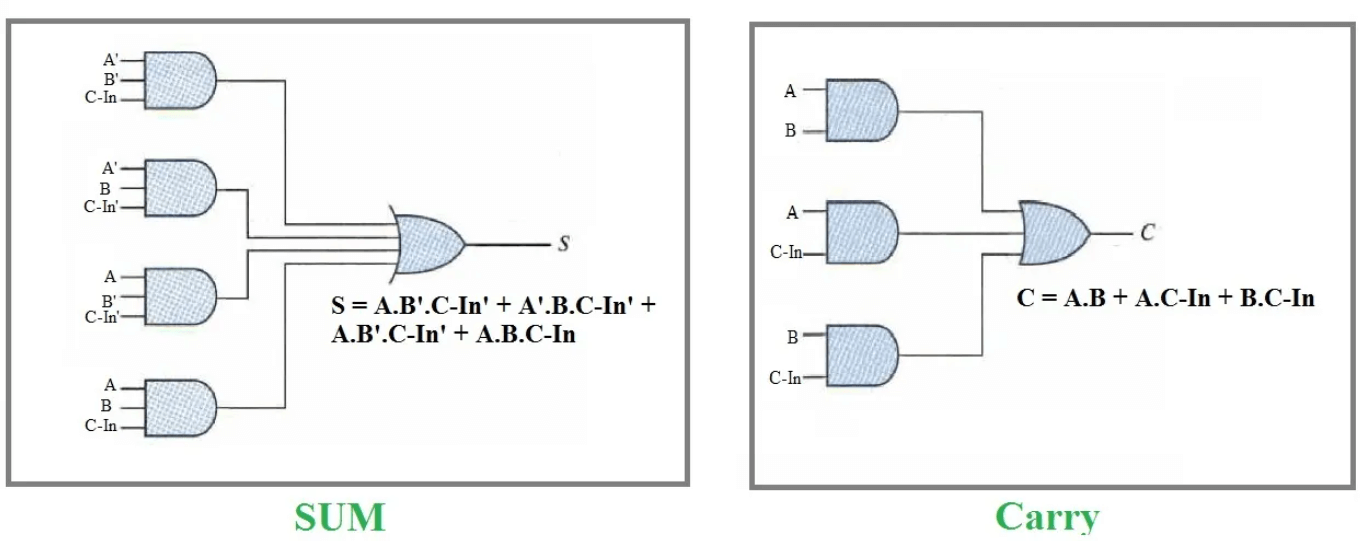
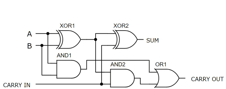
Characteristics Equations of a Full Adder
Logic Expression for SUM
Logic for COUT
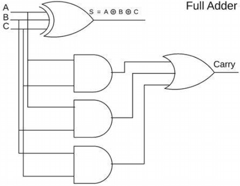
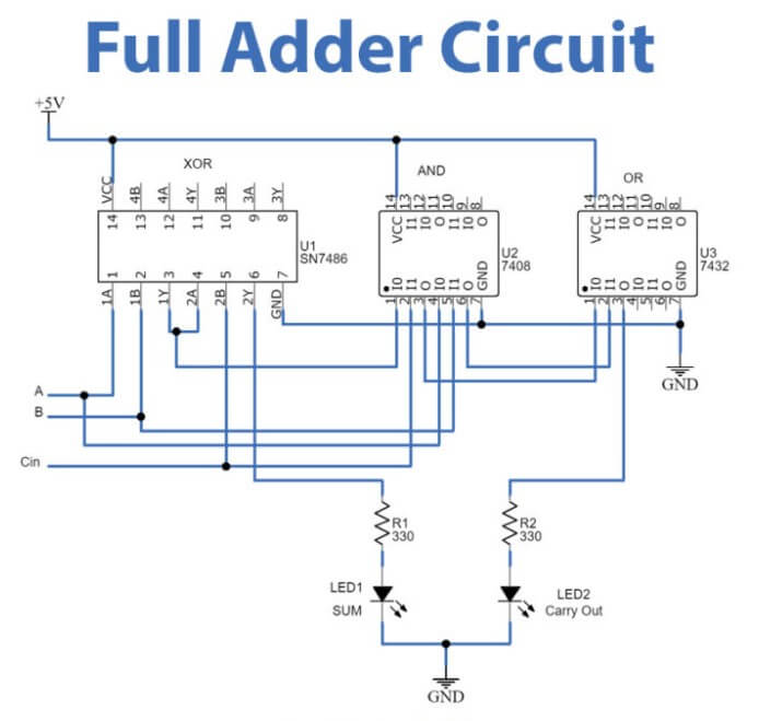
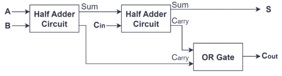
Implementing a Full Adder Circuit
Advantages and Challenges of Full Adders in Digital Logic
Advantages
Disadvantages
Applications of Full Adders in Digital Logic
Arithmetic Circuits
Data Processing
Counters
Multiplexers (MUX) and Demultiplexers (DEMUX)
Memory Technology
Arithmetic Logic Units (ALU)
Examples of Full Adder Implementations
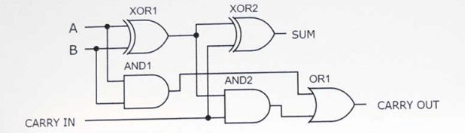
Full Adder Built with XOR, AND, and OR Gates
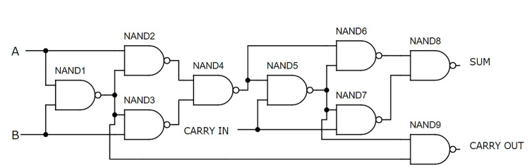
Full Adder Using NAND Gates
Full Adder with NOR Gates
Conclusion
Frequently Asked Questions [FAQ]
1. What is a full adder circuit?
2. How many AND, OR, XOR in full adder?
3. What is carry input in full adder?
4. Why use a full adder instead of a half adder?
About us
ALLELCO LIMITED
Read more
Quick inquiry
Please send an inquiry, we will respond immediately.
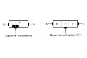
Comparison and Selection of UJT and BJT
on May 11th
Solid State Relays vs. MOSFETs Guide – Definitions, Comparisons, How to Choose
on May 10th
Popular Posts
-
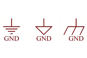
What is GND in the circuit?
on January 1th 3272
-

RJ-45 Connector Guide: RJ-45 Connector Color Codes, Wiring Schemes, R-J45 Applications, RJ-45 Datasheets
on January 1th 2815
-
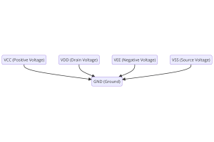
Understanding Power Supply Voltages in Electronics VCC, VDD, VEE, VSS, and GND
on November 20th 2640
-

Fiber Connector Types: SC Vs LC And LC Vs MTP
on January 1th 2265
-

Comparison Between DB9 and RS232
on January 1th 1882
-

What Is An LR44 Battery?
Electricity, that ubiquitous force, quietly permeates every aspect of our daily lives, from trivial gadgets to life-threatening medical equipment, it plays a silent role. However, truly grasping this energy, especially how to store and efficiently output it, is no easy task. It is against this background that this article will focus on a type of coin cell battery that may seem insignificant on the...on January 1th 1846
-
Understanding the Fundamentals:Inductance Resistance, andCapacitance
In the intricate dance of electrical engineering, a trio of fundamental elements takes center stage: inductance, resistance, and capacitance. Each bears unique traits that dictate the dynamic rhythms of electronic circuits. Here, we embark on a journey to decipher the complexities of these components, to uncover their distinct roles and practical uses within the vast electrical orchestra. Inductan...on January 1th 1807
-
What Is RF and Why Do We Use It?
Radio Frequency (RF) technology is a key part of modern wireless communication, enabling data transmission over long distances without physical connections. This article delves into the basics of RF, explaining how electromagnetic radiation (EMR) makes RF communication possible. We will explore the principles of EMR, the creation and control of RF signals, and their wide-ranging uses. The article ...on January 1th 1801
-
CR2430 Battery Comprehensive Guide: Specifications, Applications and Comparison to CR2032 Batteries
What is CR2430 battery ?Benefits of CR2430 BatteriesNormCR2430 Battery ApplicationsCR2430 EquivalentCR2430 VS CR2032Battery CR2430 SizeWhat to look for when buying the CR2430 and equivalentsData Sheet PDFFrequently Asked Questions Batteries are the heart of small electronic devices. Among the many types available, coin cells play a crucial role, commonly found in calculators, remote controls, and ...on January 1th 1799
-
Comprehensive guide to hFE in transistors
Transistors are crucial components in modern electronic devices, enabling signal amplification and control. This article delves into the knowledge surrounding hFE, including how to select a transistor's hFE value, how to find hFE, and the gain of different types of transistors. Through our exploration of hFE, we gain a deeper understanding of how transistors work and their role in electronic circu...on November 20th 1782
HOT Part Number
-
NTFS1205MC
Murata Power Solutions Inc.
DC DC CONVERTER 5V 1W
SN65LBC173D
Texas Instruments
IC RECEIVER 0/4 16SOIC
PAF600F24-28
TDK-Lambda Americas Inc
DC DC CONVERTER 28V 600W
MX7548JP+
Analog Devices Inc./Maxim Integrated
IC DAC 12BIT A-OUT 20PLCC
2SB0766GRL
Panasonic Electronic Components
TRANS PNP 50V 1A MINIP3-F2
S558-5999-AM-F
Bel Fuse Inc.
XFRMR MODULE LAN GIGABT MINIPCI
C0603C0G1H470J030BA
TDK Corporation
CAP CER 47PF 50V C0G 0201
CC0603GRNPO9BN471B
YAGEO
CAP CER 470PF 50V C0G/NPO 0603
AXT528124
Panasonic Electric Works
CONN SOCKET 28POS SMD GOLD
LT1763IDE-5#PBF
Analog Devices Inc.
IC REG LINEAR 5V 500MA 12DFN
MBRB4030G
onsemi
DIODE SCHOTTKY 30V 40A D2PAK
CL05B391JB5NNNC
Samsung Electro-Mechanics
CAP CER 390PF 50V X7R 0402
GRM1556T1HR50CD01D
Murata Electronics
CAP CER 0.5PF 50V T2H 0402
LM2901D
Texas Instruments
IC COMPARATOR 4 GEN PUR 14SOIC
GMJ107BB7224MAHT
Taiyo Yuden
CAP CER 0.22UF 35V X7R 0603
MIC37100-1.8BS
Microchip Technology
IC REG LINEAR 1.8V 1A SOT223-3
RT0805DRE072K1L
YAGEO
RES SMD 2.1K OHM 0.5% 1/8W 0805
744770168
Würth Elektronik
FIXED IND 68UH 2.3A 140 MOHM SMD -

XC6209F302DR-G
Torex Semiconductor Ltd
IC REG LINEAR 3V 300MA 6USPB
04023U4R3CAT2A
KYOCERA AVX
CAP CER 4.3PF 25V NP0 0402
SFECF10M8PF00-R0
Murata Electronics
FILTER 10.8MHZ SMD
MGA-31589-TR1G
Broadcom Limited
IC AMP GPS 450MHZ-1.5GHZ SOT89-3
TC4421AVPA
Microchip Technology
IC GATE DRVR LOW-SIDE 8DIP
SN74LS07DRG4
Texas Instruments
IC BUF NON-INVERT 5.25V 14SOIC
VI-J5B-IX
Vicor Corporation
DC DC CONVERTER 95V 75W
CY7C293A-20PC
Cypress Semiconductor Corp
IC EPROM 16KBIT PARALLEL
HGTD7N60C3S9A
Fairchild Semiconductor
INSULATED GATE BIPOLAR TRANSISTO
BR25G1MF-3GE2
Rohm Semiconductor
IC EEPROM 1MBIT SPI 10MHZ 8SOP
MCF51JM128EVLD
Freescale Semiconductor
IC MCU 32BIT 128KB FLASH 44LQFP
EPF10K30AQI208-3N
Intel
IC FPGA 147 I/O 208QFP
UC3835N
Texas Instruments
IC LNR REG CTRLR 1OUT 8DIP
V300A48C500BF3
Vicor Corporation
DC DC CONVERTER 48V 500W
NFM31KC103R2A3L
Murata Electronics
CAP FEEDTHRU 0.01UF 100V 1206
AOZ1340EI-1
Alpha & Omega Semiconductor Inc.
IC POWER DIST SWITCH 8MSOP
ADSP-BF518BBCZ-4
Analog Devices Inc.
IC DSP 16/32B 400MHZ 168CSBGA
TLV70730PDQNR
Texas Instruments
IC REG LINEAR 3V 200MA 4X2SON -

IRU1150CMTR
Infineon Technologies
IC REG LINEAR POS ADJ 4A TO263-5
74LS28PC
Texas Instruments
NOR GATE
06035A5R6KAT2A
KYOCERA AVX
CAP CER 5.6PF 50V NP0 0603
08051U4R7BAT2A
KYOCERA AVX
CAP CER 4.7PF 100V NP0 0805
BD7628F-E2
Rohm Semiconductor
IC AMP VIDEO 8SOP
INA166UA/2K5
Texas Instruments
IC INST AMP 1 CIRCUIT 14SOIC
FSUSB103UMX
Fairchild Semiconductor
DPDT, 2 FUNC, 2 CHANNEL
RF501PS2STB
Rohm Semiconductor
DIODE GEN PURP 200V 5A 8TSOP
AT45DB011B-XI
Microchip Technology
IC FLASH 1MBIT SPI 20MHZ 14TSSOP
SR301C334KAR
KYOCERA AVX
CAP CER RADIAL
ISL78208ARZ
Renesas Electronics America Inc
IC REG BUCK ADJ 3A DL 32QFN
170M4266
Eaton - Bussmann Electrical Division
FUSE SQUARE 630A 700VAC RECT
MBRM110ET3
onsemi
DIODE SCHOTTKY 10V 1A POWERMITE
ONET2501PARGT
Texas Instruments
IC LIMITING 1 CIRCUIT 16VQFN
HD6473827RWV
Renesas Electronics America Inc
IC MCU 8BIT 60KB OTP 80TQFP
08053C823KAJ2A
KYOCERA AVX
CAP CER 0.082UF 25V X7R 0805
74ACT14MTC
onsemi
IC INVERTER 6CH 1-INP 14TSSOP
DTC114TKAT146
Rohm Semiconductor
TRANS PREBIAS NPN 200MW SMT3