An Overview of Common-Emitter Amplifier Characteristics
Transistors, the eventual building blocks of modern electronics, serve noteworthy roles in various applications, especially as switches and amplifiers. The common-emitter configuration stands out as a versatile framework for exploiting transistors' capabilities, showcasing their utility in both analog and digital circuits. It allows precise control of devices such as lamps and motors through simple yet effective switching mechanisms. Transistors in the common-emitter setup can amplify weak signals significantly, enhancing the sensitivity and accuracy of measurement systems. This article digs into the intricate workings of transistors in the common-emitter configuration, exploring their applications in DC and AC amplification, the principles of biasing, and the impact of circuit elements on performance. Through detailed analysis, we uncover the technical nuances that make transistors requisite in modern electronic design.
Catalog
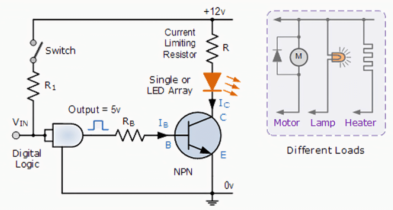
Figure 1: Transistor as a Switch
Utilizing Transistors as Efficient Simple Switches
The common-emitter configuration is a fundamental framework for transistor applications, highlighting the transistor's role as a precision switch. In this setup, the emitter is shared between the input signal and the output load, excluding the power supply. This configuration allows the transistor to efficiently control devices like lamps or motors based on the input signal's characteristics.

Figure 2: Solar Cell and Lamp
Consider a small solar cell controlling a transistor to manage a lamp's illumination. The solar cell receives varying light intensities, modulating the transistor's base current. In response, the transistor adjusts the collector current, which directly affects the lamp's brightness. By varying the base current, the transistor precisely controls the lamp's intensity, demonstrating its effectiveness as a switch.
This configuration not only showcases the transistor's basic switching function but also its utility in more sophisticated applications. For instance, it can measure light intensity, with the meter's movement driven by the solar cell's output. In low-light conditions, where the solar cell alone may not generate enough power to move the meter, the transistor amplifies the output, enhancing the system's responsiveness and effectiveness in varying ambient conditions.
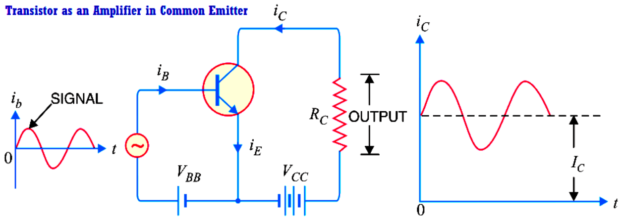
Figure 3: Transistor as an Amplifier
Optimizing Signal Strength with Transistor Amplifiers
The common-emitter configuration of a transistor is especially useful for amplifying weak signals. In this setup, the transistor boosts the small current from a solar cell, allowing for greater meter deflection with minimal light. This amplification enhances the system's sensitivity and accuracy.
The amplification is determined by the transistor's beta (β) value, which measures its current amplification factor, typically around 100. This means the meter's current is amplified to a hundred times the current produced by the solar cell. The power for this amplification comes from an external battery, ensuring the meter's readings depend only on the solar cell’s output and not the battery’s condition.
This formation shows how the transistor acts as a precise current modulator, useful in accurate measurement applications, especially those involving variable light intensities. Using the transistor in this way ensures high precision in readings and consistent performance, regardless of external power fluctuations.
Analyzing Voltage Output Across a Load Resistor
The common-emitter configuration excels at converting current input into a voltage output across a load resistor. This is particularly useful where voltage measurement is more practical than current measurement. By replacing a meter with a resistor, the circuit changes the current from a solar cell into a measurable voltage between the transistor’s collector and emitter terminals.
The transistor's operation changes with the light intensity hitting the solar cell. In darkness, the transistor stays in cutoff mode, basically off, leading to a high voltage across it. Under full light, the transistor reaches saturation, acting like a closed switch and drastically lowering the voltage drop across it.
The key aspect is that the output voltage inversely correlates with the input current, making the common-emitter configuration an inverting amplifier. This is settling for applications needing precise voltage control in response to varying input currents. SPICE simulations support this by showing the circuit’s linear performance up to the transistor's saturation point.
Exploring Transistors as AC Amplifiers
Transistors are not only effective in DC applications but are also significant for amplifying alternating current (AC) signals, a function widely used in audio electronics. Moving from simple DC switching to AC amplification requires preserving the AC signal's integrity, which is needed for applications like public address systems and audio playback devices.
• Preserving AC Signal Integrity
In AC amplification, components such as the bridge rectifier, which converts AC to DC, are omitted to maintain the AC signal's purity. This step is dynamic to avoid distortion and ensure the audio output remains undistorted.
• Maintaining Continuous Forward Bias
AC amplification in transistors is challenging due to the unidirectional nature of current flow. To keep the AC signal intact, the base-emitter junction must have a continuous forward bias. This is achieved using a bias voltage, which keeps the transistor active throughout the entire signal cycle.
• High-Fidelity Audio Reproduction
Maintaining the forward bias allows the transistor to accurately reproduce the input waveform at the output. This is noteworthy for delivering high-fidelity sound in audio applications. By ensuring the audio signal is amplified without distortion, the system provides clear and rich sound output, needed for high-quality audio systems.
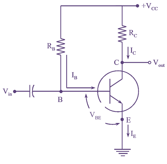
Figure 4: Transistor Biasing
Principles of Transistor Biasing
Proper biasing is required for effective transistor operation in amplification circuits, ensuring optimal signal reproduction without distortion. Biasing techniques establish a stable operating point for the transistor, typically achieved through a carefully designed resistor network. This setup allows the amplifier to deliver high-quality output consistently across the entire input signal spectrum.
Setting the correct bias voltage is serious to prevent undesirable effects like signal cutoff and distortion, which can degrade amplifier performance. Proper biasing keeps the transistor in the right operating region, ensuring consistent signal amplification under various conditions. Accurate biasing enhances the amplifier's fidelity and efficiency by providing stable operating conditions.
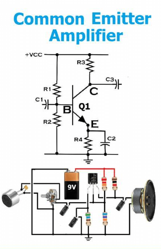
Figure 5: Common Emitter Amplifier Configuration
Mastering the Common Emitter Amplifier Configuration
The common emitter configuration is widely used in electronic circuit design for its effective amplification of both voltage and current. This setup is popular due to its strong response and compatibility with various signal types, making it compulsory in both analog and digital circuits.
In a common emitter setup, the signal is applied to the base, and the amplified output is taken from the collector, with the emitter serving as a stable reference point. This configuration significantly boosts signal strength, providing the high gain needed in many circuit designs.
The common emitter configuration is straightforward to implement and performs reliably under different conditions. Its simplicity and efficiency make it a fundamental component in electronic design. Enhancing signal strength and ensuring consistent performance, is requisite for achieving the desired amplification in numerous applications.
Analysis of the Common Emitter Amplifier
Analyzing common emitter amplifiers requires thorough AC and DC evaluations to accurately characterize their performance under various conditions. This analysis ensures the amplifier operates efficiently and reliably in practical applications.
The analysis starts with DC evaluation, where biasing conditions are established. This determines the operating point, ensuring linear amplification without distortion. Proper biasing is insistent to set the transistor in the correct region of operation.
Next, AC analysis is performed by deactivating all DC sources and using the transistor's small-signal equivalent model. This helps predict the amplifier's behavior over a range of frequencies.
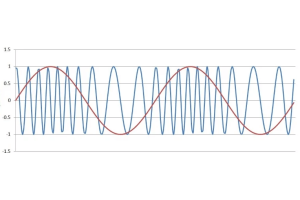
Frequency Response of the CE Amplifier
The frequency response of a common emitter (CE) amplifier is a testing metric that shows how the amplifier performs across different signal frequencies. It highlights variations in voltage gain due to capacitive effects within the circuit. This is particularly imperative for designing amplifiers, such as audio amplifiers, that need consistent performance over a specified frequency range.
To analyze frequency response, engineers plot the voltage gain against frequency. This graph delineates the amplifier's bandwidth and characterizes its performance at low, mid, and high frequencies. The resulting plot provides a detailed understanding of the amplifier’s operational efficacy. It reveals any frequency-dependent limitations or enhancements, offering insights that are invaluable for tailoring the amplifier to specific applications.
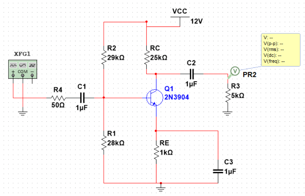
Figure 6: Voltage Gain in Common Emitter Amplifiers
Understanding Voltage Gain in Amplifiers
Voltage gain in common emitter amplifiers is a significant metric. It is measured by comparing the output voltage amplitude to the input voltage amplitude, after accounting for any DC offsets. This measurement is dynamic in applications like audio amplification, where maintaining signal integrity and fidelity is a must.
The design of the amplifier circuit, especially the resistance values for the input and load, significantly affects the voltage gain. Selecting and tuning these resistors carefully is the principal to achieve the desired amplification levels. Proper management of these parameters ensures the amplifier delivers the required voltage gain without compromising signal quality. Careful calibration of the resistance values maintains the balance between amplification power and audio quality.
Overview of Circuit Elements and Their Roles
In a common emitter amplifier circuit, each component has a specific role that impacts the overall performance. Key elements include bias resistors, capacitors, and the transistor, each testing for the circuit's functionality.
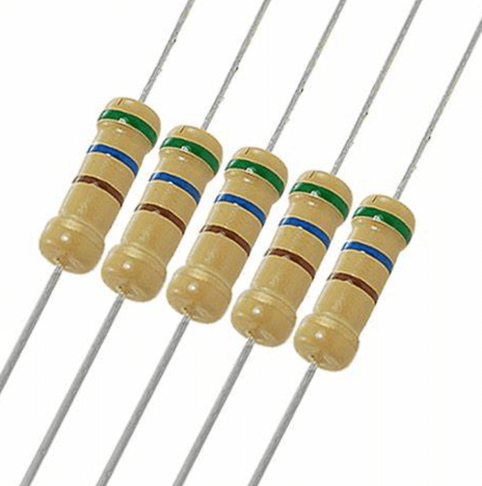
Figure 7: Bias Resistors
Bias resistor sets the operating point of the transistor, ensuring it is in its active region. This allows for linear amplification without distortion.
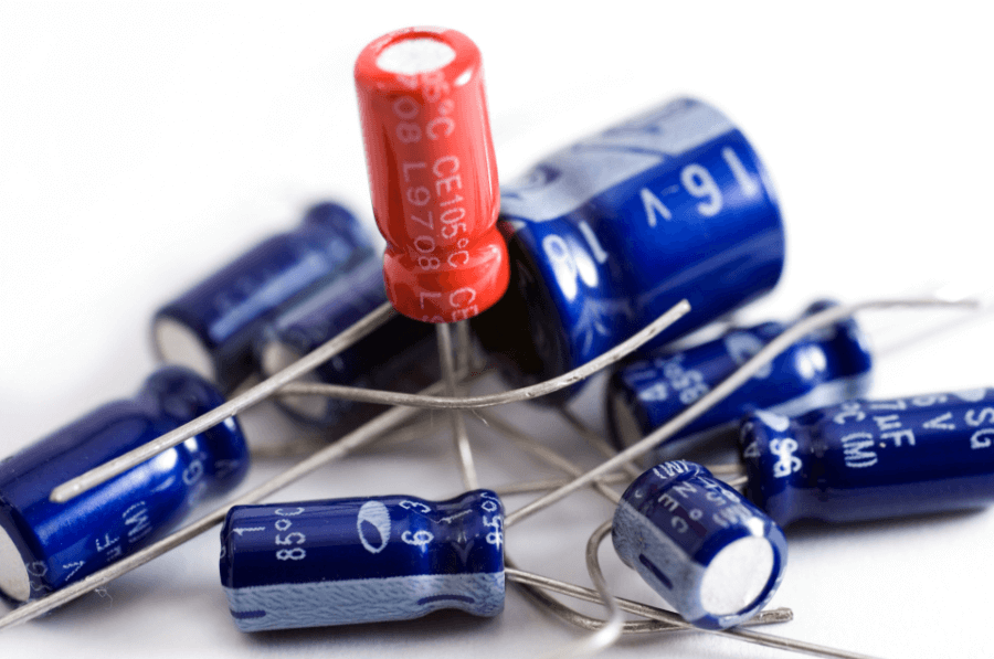
Figure 8: Capacitors
Capacitors are used for signal coupling and decoupling. They block DC components while allowing AC signals to pass, preserving the integrity of the amplified signal.

Figure 9: Transistor
The transistor is the core component of the amplifier. It acts as the active element for signal amplification. The transistor's characteristics, such as current gain and response speed, directly affect the amplifier's output quality.
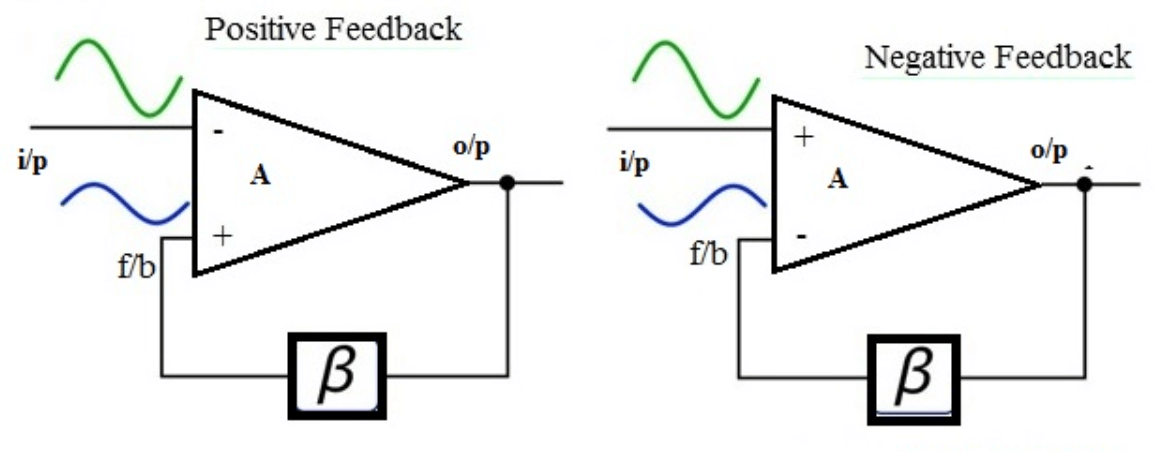
Figure 10: Amplifier Feedback Mechanism
Implementing Feedback Mechanisms in Amplifiers
Feedback mechanisms are influential in amplifiers, as they modulate output characteristics by reintroducing part of the output back into the input. This can stabilize or destabilize the amplifier, depending on the type of feedback used.
Positive feedback amplifies the input signal, which can enhance performance in applications like oscillators. However, if not carefully managed, it can cause unwanted oscillations and make the amplifier unstable.
Negative feedback reduces distortions and stabilizes the amplifier by opposing the input signal. It improves linearity, reduces noise, and increases bandwidth, making the amplifier more reliable.
Effective feedback management is deciding to optimize amplifier performance. Engineers must design the feedback network to balance amplification, stability, and bandwidth. Proper feedback design prevents issues like feedback-induced noise or distortion and ensures efficient operation within the intended application.
Evaluating Input and Output Impedance in Common Emitter Amplifiers
The input and output impedance of a common-emitter amplifier is a very important factor for its performance and integration in an electronic system.

Figure 11: Input Impedance
The input impedance is typically low in common emitter configurations. This low impedance facilitates the easier acquisition of signals from preceding stages, ensuring effective signal transfer without significant loss or loading effects.
Figure 12: Output Impedance
In difference, the output impedance is usually high in this configuration. The high output impedance is beneficial for driving subsequent stages, acting as a buffer that minimizes interaction between the amplifier and the load.
Properly managing these impedances is needed for optimal amplification. It ensures high-quality signal integrity and compatibility with various components, from the signal source to the final output stages.
The Function of Coupling Capacitors in Amplifiers
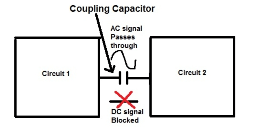
Figure 13: Coupling Capacitors in Electronic Circuits
In electronic circuits, particularly in Common Emitter Amplifier setups, coupling capacitors C1 and C2 play a powerful role. These capacitors are designed to separate alternating current (AC) signals from direct current (DC) biasing voltages. This separation is influential for maintaining the circuit's bias conditions unchanged during amplification. Coupling capacitors allow AC signals to pass through while blocking DC components. This ensures that the AC output from one amplification stage transitions smoothly to the next stage without affecting the bias settings.
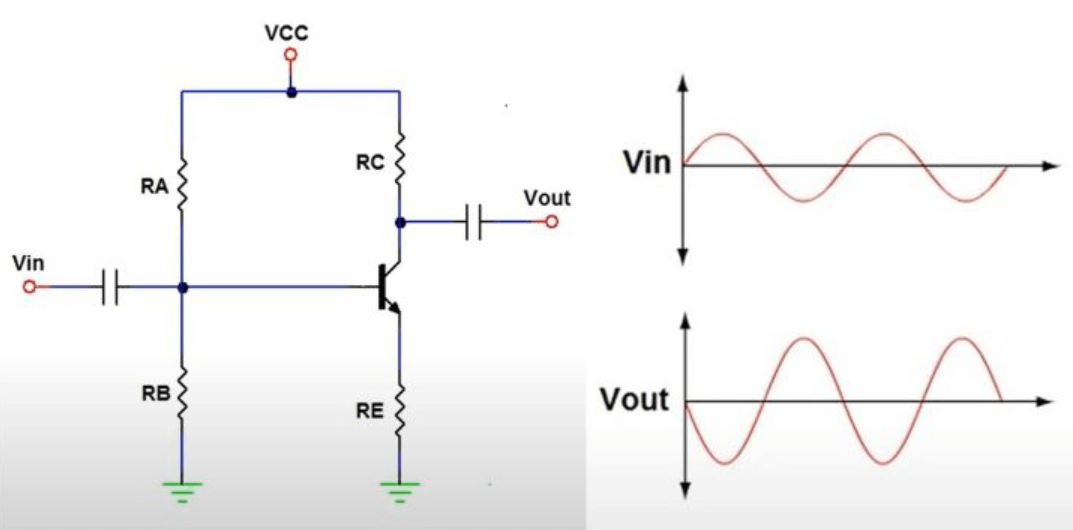
Figure 14: Bypass Capacitor for Circuit Stability
A bypass capacitor, labeled CE, is included in the emitter path to enhance circuit stability. Under DC conditions, CE acts as an open circuit, leaving bias currents and voltages unaltered. This is requisite for maintaining the operational quiescent point (Q-point) stable throughout the circuit's operation. However, at higher frequencies, CE shunts the emitter resistor, significantly lowering its reactance. This reduction in reactance decreases the overall impedance faced by the AC signal, focusing it primarily on the load resistor, RL, and a minimal internal resistance. This optimizes the voltage gain of the amplifier.
The value of CE is risky for the amplifier's performance. It is typically chosen so that its reactance is significantly lower, ideally less than one-tenth of the emitter resistor, RE, at the lowest operational frequency. This selection enhances the amplifier's high-frequency response, ensuring efficient performance across a wide range of frequencies.
Advantages of Modern Electronic Components
The common emitter amplifier configuration is a cornerstone in electronics due to its unique advantages. It has a low input impedance, making it ideal as an inverting amplifier. What’s more, its high output impedance is advantageous for impedance matching, thereby improving system compatibility and performance.
• Exceptional Power and Current Gain
One of the most notable benefits of common emitter amplifiers is their exceptional power gain, which is the highest among amplifier configurations when balanced with voltage and current gains. This high-power gain is paired with significant current gain, enhancing its effectiveness in applications that require strong current amplification. This combination of high power and current gains makes the common emitter amplifier valuable in a wide range of both general and specialized electronic applications.
• Versatility and Efficiency
The versatility and efficiency of the common emitter amplifier make it useful in circuits that handle complex signal processing and amplification tasks. Its ability to provide substantial power and current gains ensures it can meet diverse amplification needs, making it a settling component in many electronic systems.
Disadvantages of Contemporary Electronic Designs
Common emitter amplifiers, though dynamic in many electronic applications, face significant limitations at high frequencies. As the frequency increases, their performance drops, making them less suitable for tasks that need wide bandwidth or stable high-frequency operations.
• Voltage Gain Instability
Another issue is the inherent instability of their voltage gain. This instability makes it difficult to maintain consistent performance under varying operational conditions.
• High Output Resistance
Common emitter amplifiers also have a high output resistance. This characteristic complicates their integration with subsequent circuit stages, as it requires careful impedance matching to ensure efficient signal transmission.
• Thermal Instability
Thermal instability is a serious drawback. These amplifiers need robust thermal management to maintain reliable performance, especially in environments with fluctuating or extreme temperatures.
Applications of Transistor-Based Technologies
|
Applications of Transistor-Based Technologies |
|
|
Low-Frequency Voltage Amplification
|
Common emitter amplifiers are highly versatile and influential in many electronic applications. They excel in low-frequency voltage amplification, efficiently handling signals below the RF spectrum with minimal loss. This makes them ideal for audio applications and other tasks requiring stable, low-frequency signal processing.
|
|
Role in RF Circuits
|
In radio frequency (RF) circuits, common emitter amplifiers are vigorous for enhancing signal strength and quality. They are often used to amplify weak signals to usable levels, playing a key role in RF signal processing.
|
|
Low Noise Amplifiers
|
These amplifiers are also analytical in low-noise applications, where high signal integrity and minimal distortion are needed. They are commonly found in sensitive communication and measurement equipment, ensuring precise and reliable signal amplification.
|
|
RF Transceiver Circuits
|
Common emitter amplifiers are requisite in RF transceiver circuits for both signal transmission and reception. They ensure robust and reliable communication in various telecommunications applications |
Conclusion
In conclusion, the common-emitter transistor configuration stands as a cornerstone in the realm of electronic design, offering unparalleled benefits in amplifying and switching applications due to its robust response and compatibility with a variety of signal types. The article has systematically unpacked the operational principles and practical applications of this configuration, from its ability to enhance low-frequency voltage amplification to its unsafe use in RF circuits.
Despite facing challenges like high-frequency limitations and thermal instability, the common-emitter amplifier remains mandatory in modern electronics. Its ability to maintain signal integrity, coupled with the versatility to adapt across a broad spectrum of operational conditions, underscores its key role in advancing electronic technology and optimizing circuit performance for both everyday and specialized tasks.
Frequently Asked Questions [FAQ]
1. What is a common emitter amplifier using a PNP transistor?
A common emitter amplifier with a PNP transistor is a type of amplifier circuit where the emitter of the PNP transistor is connected commonly to both the input and the output of the circuit. This configuration amplifies the input signal at the base, resulting in a larger output signal at the collector. In a PNP transistor setup, the current flows from the emitter to the collector when a negative voltage is applied to the base relative to the emitter.
2. How does the common emitter amplifier change the phase?
In a common emitter amplifier, the output signal is phase-inverted, meaning it is 180 degrees out of phase with the input signal. This occurs because the input signal's variations cause inverse variations in the emitter current, which, due to transistor properties, lead to opposite changes in the collector voltage. Thus, when the input signal goes up, the output voltage goes down, and vice versa.
3. How do you identify an emitter in a transistor?
To identify the emitter of a transistor, look for the lead connected to the semiconductor material with the highest doping concentration. The emitter typically has a thicker arrow in the symbol for bipolar junction transistors, pointing away from the base in an NPN transistor and toward the base in a PNP transistor. Checking the datasheet for the specific transistor model is also recommended, as it will provide the exact pin configuration.
4. What is the difference between the emitter and collector of a transistor?
The main difference lies in their function and construction within the transistor. The emitter is heavily doped to inject carriers into the base, while the collector is moderately doped and designed to collect these carriers. This difference in doping levels means the emitter can release more charge carriers compared to the collector, which is optimized to collect and remove these carriers from the base.
5. Why is the CE amplifier mostly used?
The common emitter (CE) amplifier is widely used due to its ability to provide a good balance of gain, efficiency, and impedance characteristics. It offers significant voltage gain and reasonable linearity, making it suitable for a variety of applications in signal amplification. In addition, its phase inversion capability is useful in signal-processing circuits, and its relatively simple configuration makes it easy to implement in both discrete and integrated circuit designs.
About us
ALLELCO LIMITED
Read more
Quick inquiry
Please send an inquiry, we will respond immediately.
Dual Inline Package (DIP): An Overview
on June 27th
The Impact of Harmonics on Electrical Systems
on June 25th
Popular Posts
-
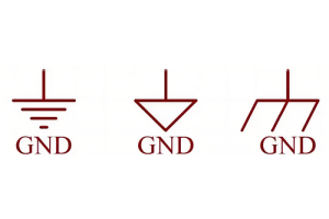
What is GND in the circuit?
on January 1th 2938
-

RJ-45 Connector Guide: RJ-45 Connector Color Codes, Wiring Schemes, R-J45 Applications, RJ-45 Datasheets
on January 1th 2501
-

Fiber Connector Types: SC Vs LC And LC Vs MTP
on January 1th 2089
-
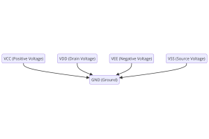
Understanding Power Supply Voltages in Electronics VCC, VDD, VEE, VSS, and GND
on November 9th 1893
-

Comparison Between DB9 and RS232
on January 1th 1764
-

What Is An LR44 Battery?
Electricity, that ubiquitous force, quietly permeates every aspect of our daily lives, from trivial gadgets to life-threatening medical equipment, it plays a silent role. However, truly grasping this energy, especially how to store and efficiently output it, is no easy task. It is against this background that this article will focus on a type of coin cell battery that may seem insignificant on the...on January 1th 1713
-
Understanding the Fundamentals:Inductance Resistance, andCapacitance
In the intricate dance of electrical engineering, a trio of fundamental elements takes center stage: inductance, resistance, and capacitance. Each bears unique traits that dictate the dynamic rhythms of electronic circuits. Here, we embark on a journey to decipher the complexities of these components, to uncover their distinct roles and practical uses within the vast electrical orchestra. Inductan...on January 1th 1655
-

CR2430 Battery Comprehensive Guide: Specifications, Applications and Comparison to CR2032 Batteries
What is CR2430 battery ?Benefits of CR2430 BatteriesNormCR2430 Battery ApplicationsCR2430 EquivalentCR2430 VS CR2032Battery CR2430 SizeWhat to look for when buying the CR2430 and equivalentsData Sheet PDFFrequently Asked Questions Batteries are the heart of small electronic devices. Among the many types available, coin cells play a crucial role, commonly found in calculators, remote controls, and ...on January 1th 1554
-
What Is RF and Why Do We Use It?
Radio Frequency (RF) technology is a key part of modern wireless communication, enabling data transmission over long distances without physical connections. This article delves into the basics of RF, explaining how electromagnetic radiation (EMR) makes RF communication possible. We will explore the principles of EMR, the creation and control of RF signals, and their wide-ranging uses. The article ...on January 1th 1539
-

CR2450 vs CR2032: Can The Battery Be Used Instead?
Lithium manganese batteries do have some similarities with other lithium batteries. High energy density and long service life are the characteristics they have in common. This kind of battery has won the trust and favor of many consumers because of its unique safety. Expensive tech gadgets? Small appliances in our homes? Look around and you'll see them everywhere. Among these many lithium-manganes...on January 1th 1512
HOT Part Number
-
UCC2580DTR-4
Texas Instruments
IC OFFLINE SW MULT TOP 16SOIC
1N3015RB
Microchip Technology
DIODE ZENER 200V 10W DO213AA
TNETE2008PBE
Texas Instruments
OBSOLETED - LTB ENDS 07-25-2000
24LC32A/P
Microchip Technology
IC EEPROM 32KBIT I2C 400KHZ 8DIP
BC859CLT1G
onsemi
TRANS PNP 30V 0.1A SOT23-3
IPP80N06S2-H5
Infineon Technologies
IPP80N06 - 55V-60V N-CHANNEL AUT
VE-JW3-MZ
Vicor Corporation
DC DC CONVERTER 24V 25W
SSM2302CPZ-REEL7
Analog Devices Inc.
IC AMP CLASS D STER 1.4W 16LFCSP
12063A222JAT2A
KYOCERA AVX
CAP CER 2200PF 25V NP0 1206
GRM1885C1H2R0BA01D
Murata Electronics
CAP CER 2PF 50V C0G/NP0 0603
AD5422BREZ-REEL
Analog Devices Inc.
IC DAC 16BIT V OR A-OUT 24TSSOP
DS2114Z
Analog Devices Inc./Maxim Integrated
IC TERM SCSI 2% 150MIL 16-SOIC
LB8112V-TLM-E
onsemi
SYSTEM MOTOR DRIVER
954206AGLFT
Renesas Electronics America Inc
IC TIMING CTRL HUB P4 56-TSSOP
5962-9681001QXA
Texas Instruments
3.3V ABT 16-BIT TRANSPARENT D-TY
ADSP-1016AKN
Analog Devices Inc.
16 X 16 CMOS MULTIPLIER
RK73H2BTTD1212F
KOA Speer Electronics, Inc.
RES 12.1K OHM 1% 1/4W 1206
CY7C1518KV18-333BZXC
Infineon Technologies
IC SRAM 72MBIT PARALLEL 165FBGA -
AD829JR
Analog Devices Inc.
IC AMP VOLTAGE FEEDBACK 8SOIC
LX1675CLQ-TR
Microsemi Corporation
IC REG QUAD BUCK/LNR SYNC 38MLPQ
SZBZX84C47LT1G
onsemi
DIODE ZENER 47V 225MW SOT23-3
UDZLVTE-1791
Rohm Semiconductor
DIODE ZENER 91V 200MW SOD323FL
ACS108-5SN
STMicroelectronics
TRIAC SENS GATE 500V 0.8A SOT223
SRR5028-120Y
Bourns Inc.
FIXED IND 12UH 1.46A 80 MOHM SMD
SMM02070C1690FBS00
Vishay Beyschlag/Draloric/BC Components
RES SMD 169 OHM 1% 1W MELF
P6SMB440A
Meritek
TVS DIODE 376.2VWM 607.2VC
1808GC102KATRE
KYOCERA AVX
CAP CER 1000PF 2KV X7R 1808
1850BL15B050E
Johanson Technology
BALUN 1.7GHZ-2GHZ 50/50 0805
LT3741IFE-1#TRPBF
Analog Devices Inc.
IC REG CTRLR BUCK 20TSSOP
SD25-0836R9UBM1
KYOCERA AVX
DUPLEXER SAW 8SMD
MBC13720NT1
Freescale Semiconductor
SiGe:C Low Noise Amplifier with
LM285LP-1-2
Texas Instruments
IC VREF SHUNT 1% TO92-3
UA78L15ACLPR
Texas Instruments
IC REG LINEAR 15V 100MA TO92-3
AT87C51RB2-3CSUM
Atmel
IC MCU 8BIT 16KB OTP 40PDIL
TPS51225BRUKR
Texas Instruments
IC REG QUAD BUCK/LNR SYNC 20WQFN
ADS1282IPWR
Texas Instruments
IC ADC 31BIT SIGMA-DELTA 28TSSOP -
MAX4491AUA
Analog Devices Inc./Maxim Integrated
IC OPAMP GP 2 CIRCUIT 8UMAX
MSP430F1612IPM
Texas Instruments
IC MCU 16BIT 55KB FLASH 64LQFP
08054W106MAT2A
KYOCERA AVX
CAP CER 10UF 4V X6S 0805
12102C103JAT2A
KYOCERA AVX
CAP CER 10000PF 200V X7R 1210
RLZTE-115.6A
Rohm Semiconductor
DIODE ZENER 5.6V 500MW LLDS
AD8613AKSZ-REEL7
Analog Devices Inc.
IC OPAMP GP 1 CIRCUIT SC70-5
MPXV4006GC6U
NXP USA Inc.
SENSOR 0.87PSIG 0.13" 4.7V
LCMXO2-2000HE-6MG132I
Lattice Semiconductor Corporation
IC FPGA 104 I/O 132CSBGA
CRCW060356R0FKEA
Vishay Dale
RES SMD 56 OHM 1% 1/10W 0603
SIB437EDKT-T1-GE3
Vishay Siliconix
MOSFET P-CH 8V 9A PPAK TSC75-6
BQ29442DRBR
Texas Instruments
IC BATT PROT LI-ION 2-4CELL 8SON
SLI-343D8U3F
Rohm Semiconductor
LED ORANGE DIFFUSED T-1 T/H
CC1206KRX7R0BB563
YAGEO
CAP CER 0.056UF 100V X7R 1206
TPS61161ADRVR
Texas Instruments
IC LED DRV RGLTR PWM 700MA 6WSON
TPS79628DCQ
Texas Instruments
IC REG LINEAR 2.8V 1A SOT223-6
PTH12010YAD
Artesyn Embedded Power
DC DC CONVERTER 0.55-1.8V 27W
FDU6688
Fairchild Semiconductor
MOSFET N-CH 30V 84A IPAK
NN30331A-VB
Panasonic Electronic Components
IC REG BUCK ADJUSTABLE 8A 24QFN