Dual Inline Package (DIP): An Overview
In the world of electronics, how we package and connect tiny computer chips, called integrated circuits (ICs), is very important. One packaging type that has been used for a long time is the Dual Inline Package, or DIP for short. This type of packaging has two rows of metal pins that make it easy to connect the chip to other parts. DIP packages are easy to use and reliable, which is why they have been popular for many years. In this article, we will look at what DIP packaging is, the different types of DIPs, their history, how they are made, and how they compare to newer packaging types like SOIC. Whether you're an experienced electronics engineer or just curious about how electronics work, understanding DIP packaging is very helpful.
Catalog
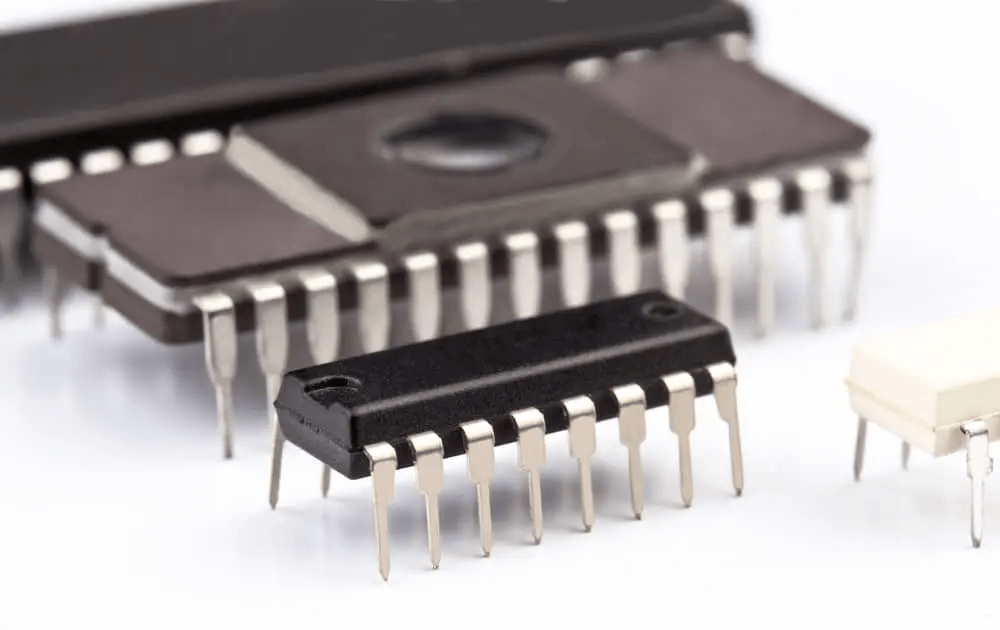
Figure 1: Dual Inline Package (DIP)
What Is Dual Inline Package?
A Dual Inline Package (DIP) is a type of integrated circuit (IC) packaging that has two rows of metal pins on the sides of a rectangular case. These pins connect the IC to a circuit board, either by soldering directly onto a printed circuit board (PCB) or by insertion into a DIP socket for easy removal. DIP packages are widely used for various electronic components, including ICs, switches, LEDs, seven-segment displays, bar graph displays, and relays. Their design makes assembly easy and ensures reliable connections. The structure consists of a rectangular chip case with two rows of evenly spaced pins, which simplifies PCB design and layout. This setup allows for secure connections when mounted on a PCB.
DIP packaging offers benefits such as ease of soldering and assembly, suitable for both manual and automated processes. It provides good heat dissipation, which is important for maintaining the performance and lifespan of electronic components. The dual in-line arrangement allows for easy replacement of components without damaging the surrounding circuitry, making DIP packages ideal for prototyping and frequent component swapping. Although largely replaced by surface mount technology (SMT) in modern electronics, DIP remains valuable for its durability, ease of handling, and straightforward assembly. The consistent pin arrangement and strong design of DIP packages continue to support their use in various electronic applications.
Types of Dual Inline Packages
Dual Inline Package (DIP) technology includes several types, each with special features and uses. These types are made to meet different needs and work well in various situations.
Ceramic DIP (CDIP)
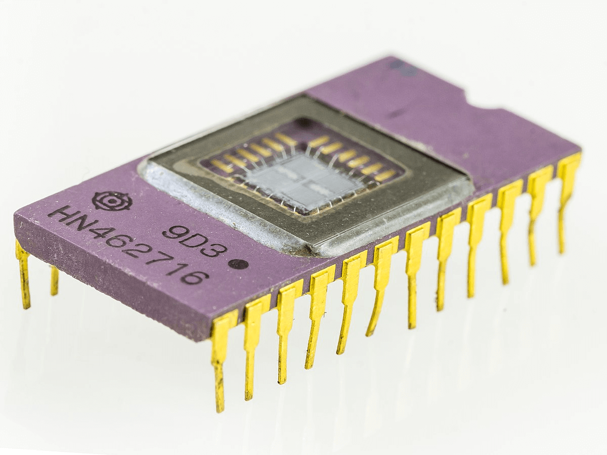
Figure 2: Ceramic Ceramic DIP
Ceramic DIPs are known for their excellent electrical performance and strong resistance to heat, moisture, and shock. The ceramic material reduces interference with electrical signals, making CDIPs great for high-frequency uses. The toughness of ceramic also makes these packages very durable and good for tough environments with extreme temperatures and humidity.
Plastic DIP (PDIP)
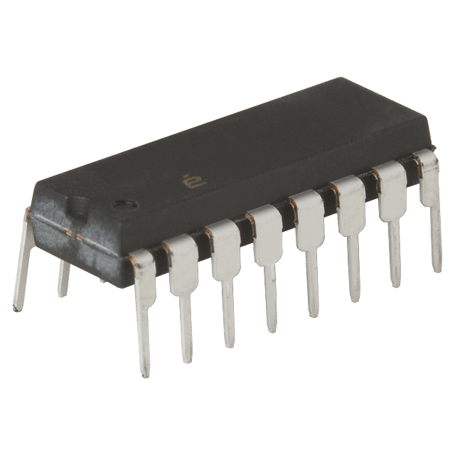
Figure 3: Plastic DIPs
Plastic DIPs have two parallel rows of pins that provide stable connections to the integrated circuit (IC). The plastic material offers good insulation, protecting the IC from outside factors and preventing electrical shorts. PDIPs are widely used in consumer electronics because they are cost-effective and provide enough protection for most uses.
Shrink Plastic DIP (SPDIP)
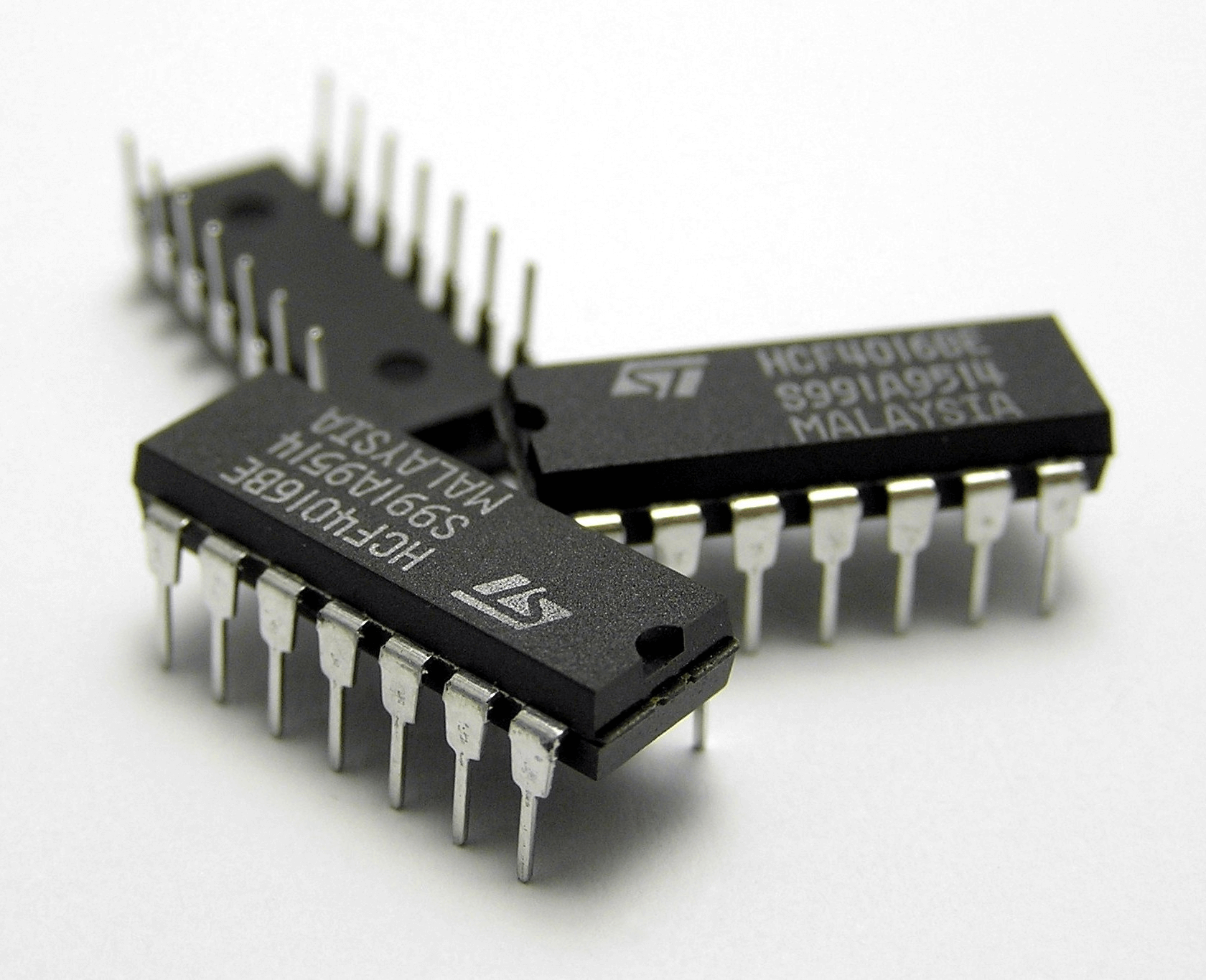
Figure 4: Shrink Plastic DIPs
Shrink Plastic DIPs are designed to save space on circuit boards by having a smaller lead pitch of 0.07 inches (1.778mm). This smaller pitch allows for a denser arrangement of parts on the board, making SPDIPs very useful in small electronic devices where space is limited. Despite the smaller size, SPDIPs keep the strength of electrical connections and the protective properties of plastic DIPs.
Skinny DIP (SDIP)
Figure 5: Skinny DIPs
Skinny DIPs are notable for their smaller width of 7.62mm and a pin center distance of 2.54mm. This smaller size is helpful in applications needing a narrow package to fit within tight spaces on a circuit board. The consistent pin spacing ensures they can be easily used with standard through-hole mounting techniques, fitting into existing designs without needing special changes.
Each type of DIP package is designed to meet specific needs, from being extra durable in tough environments to saving space in small devices. By understanding the unique features and uses of each DIP type, designers can choose the best packaging for their integrated circuits, ensuring they work well and last a long time in their electronic systems.
Evolution of DIP Package
The Dual Inline Package (DIP) was created by Bryant Buck Rogers of Fairchild Semiconductor in 1964. It introduced a rectangular housing with two rows of pins, changing how integrated circuits (ICs) connected to circuit boards. The first DIP had 14 pins, a design still used today.
The rectangular shape of the DIP allows more components to be mounted on a circuit board, making it ideal for developing smaller, more complex devices. Its two rows of pins make connection to the PCB more reliable and easier.
DIP packaging was ideal for automated assembly, allowing many ICs to be mounted and soldered at once using wave soldering. This reduced time and labor. It also suited automated testing, ensuring high reliability and quality control.
The invention of the DIP streamlined manufacturing and enabled the development of advanced electronic devices, influencing future packaging innovations and leading to the miniaturization of integrated circuits.
In the 1970s and 1980s, DIP was the main packaging for microelectronics due to its simplicity and through-hole mounting. The need for smaller, more efficient, and higher-density components led to the development of surface mount technology (SMT) in the 21st century. SMT packages, like PLCC and SOIC, mounted directly onto PCB surfaces, allowing for compact, lightweight designs without drilling holes.
SMT provided better performance due to shorter lead lengths but posed challenges for manual handling and soldering. Adapters were created to use SMT components in DIP setups, combining compactness with ease of use.
DIP components were once popular for programmable parts due to easy programming via external equipment. However, in-line programming (ISP) technology reduced the need for DIP's easy programming. The industry shifted to SMT, which supports ISP and offers many benefits.
By the 1990s, SMT began to replace DIP, especially for components with more than 20 pins. SMT components are smaller, lighter, and better for high-density designs, enabling efficient automated assembly. This trend continued into the 21st century, with new components designed mainly for SMT.
DIP packages became less common due to their bulky size and larger footprint. They are less appealing for modern, space-efficient applications and have mechanical and thermal weaknesses. However, they are still used for prototyping and educational purposes due to their ease of handling and use in breadboards. The shift to SMT reflects the industry's move towards more advanced, compact, and efficient designs.
DIP Structure

Figure 6: DIP (Dual Inline Package) Structure
A DIP (Dual Inline Package) has several important parts:
Leadframe
The leadframe is a thin metal frame that holds the silicon die and connects it to the outside world. Usually made from copper or a copper alloy, the leadframe is picked because it conducts electricity well and is strong. It has many metal pins that will connect to the circuit board. These pins make sure that electrical signals can move easily between the silicon die and the external circuits.
Package Substrate
The package substrate is a thin piece of insulating material that supports and separates the leadframe and the silicon die. Made from materials like epoxy resin or plastic, the substrate is chosen for its insulating properties and durability. It makes sure that electrical connections are stable and separate, preventing short circuits and other electrical problems.
Silicon Die
The most important part of the DIP package is the silicon die, which contains the electronic circuits that make the IC work. This die is a small piece of silicon, carefully crafted and treated with various elements to create the transistors, diodes, resistors, and other parts used in the IC's operation. The silicon die is usually attached to the leadframe using an adhesive, providing stability and good heat conduction.
Gold Wirebonds
To connect the silicon die to the leadframe, gold wirebonds are used. These thin gold wires are attached to the contact points on the silicon die and the matching points on the leadframe. Gold is used because it conducts electricity well and does not rust, ensuring reliable electrical connections throughout the device's life. The wirebonding process is very important, as it creates the paths through which electrical signals travel between the silicon die and the outside world.
Polymer Overmold
The polymer overmold is a protective coating that covers the leadframe, package substrate, silicon die, and gold wirebonds. This overmold is usually made from an epoxy or plastic compound, chosen for its protective qualities. The overmold provides mechanical protection, shielding the delicate internal components from physical damage and environmental factors like moisture and dust. It also helps to keep out contaminants that could affect the IC's performance.
Pros and Cons of Dual Inline Package
Pros
One of the main benefits of the Dual Inline Package (DIP) is its simplicity and low cost. The basic design of DIP packages makes them easy to make, which helps keep production costs low. This simplicity also extends to the assembly process, as DIP components work well with through-hole mounting techniques. This process involves placing component leads into holes on a printed circuit board (PCB) and soldering them in place. This method works well for both manual and automated assembly lines, making DIP ideal for large-scale production.
Another useful feature of DIP packages is their good heat management. The through-hole design allows heat produced by the component to spread out more effectively into the PCB, which helps keep the circuit reliable and long-lasting. Also, DIP components are easy to replace without damaging nearby parts. This is particularly handy for prototyping and testing, where components may need to be swapped out often.
Cons
Despite these benefits, there are some downsides to using DIP packages. One of the main drawbacks is the amount of space they take up on the circuit board. Compared to surface-mount technology (SMT) packages, DIP components are larger and occupy more space on the PCB. This makes them less suitable for applications where space is limited or where a high number of components need to fit in a small area.
DIP packages are also not the best choice for high-density applications because of their limited pin spacing. The standard 0.1-inch (2.54 mm) distance between pins limits the number of connections that can be made within a given area. This can be a major issue for complex circuits that require many connections in a small space.
Pins of DIP

Figure 7: Pins of a 40-pin DIP (Dual In-line Package)
DIP parts have standard sizes that follow JEDEC rules. The space between two pins (called pitch) is 0.1 inches (2.54 mm). The space between two rows of pins depends on how many pins are in the package. Common row spacings are 0.3 inches (7.62 mm) or 0.6 inches (15.24 mm). The number of pins in a DIP package is always an even number, ranging from 8 to 64.
Electrical Characteristics of DIP Components
Dual Inline Package (DIP) components have certain electrical features that affect how well they work and how long they last.
• Electrical Life: These parts are tested for 2000 on-off cycles at 24 volts DC and 25 milliamps. This test makes sure they are strong and reliable over time.
• Rated Current: For switches used less often, they can handle up to 100 milliamps with a voltage of 50 volts DC. For switches used more often, they can handle 25 milliamps with a voltage of 24 volts DC.
• Contact Resistance: When new, the contact resistance should not be more than 50 milliohms. After testing, it should not go over 100 milliohms. This measures how much resistance is at the contact points.
• Insulation Resistance: This should be at least 100 megohms at 500 volts DC. This high resistance prevents unwanted current flow between different parts.
• Withstand Voltage: These components can handle up to 500 volts AC for one minute. This means they can survive sudden increases in voltage without failing.
• Inter-Electrode Capacitance: This should not be more than 5 picofarads. Low capacitance helps to reduce interference and keeps signals clear, especially in high-frequency uses.
• Circuit Configurations: DIP components come in different types such as single-pole, single-throw (SPST) and double-pole, double-throw (DPDT). This gives more options for controlling circuits in different designs.
DIP vs SOIC
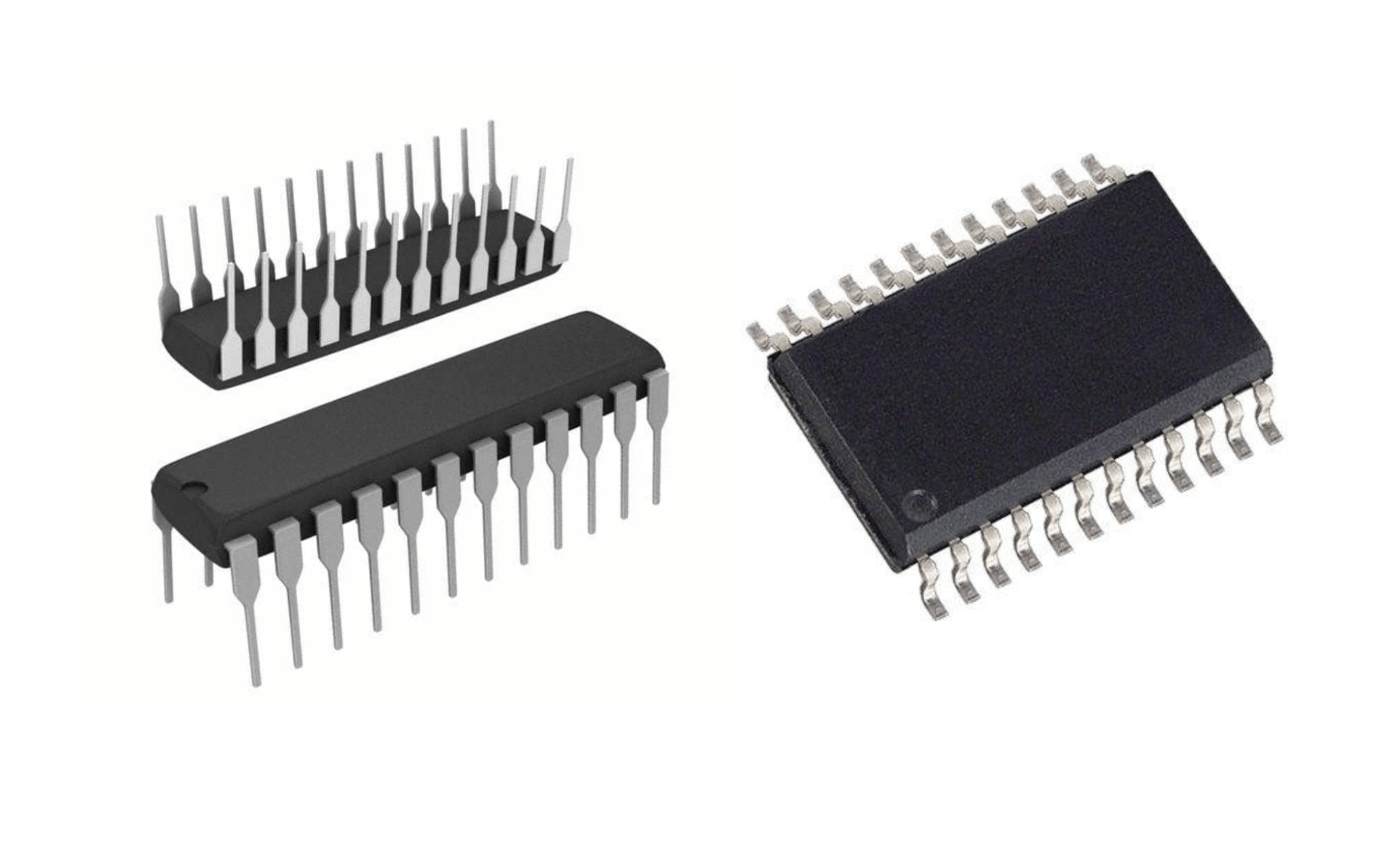
Figure 8: DIP (Dual In-line Package) and SOIC (Small Outline Integrated Circuit)
Dual In-line Package (DIP) and Small Outline Integrated Circuit (SOIC) are two common types of packaging for integrated circuits (ICs). Each type has different features that make it suitable for certain uses, and knowing these differences helps in choosing the right package for an electronic design.
DIP, or dual in-line package, has two rows of metal pins extending from each side of a rectangular plastic or ceramic body. These pins can be soldered directly onto a printed circuit board (PCB) through drilled holes or inserted into a socket. The DIP design is ideal for through-hole mounting, which involves placing component leads into holes drilled into the PCB and soldering them on the other side. This method provides strong connections and is good for applications needing durable and robust connections.
In contrast, SOIC, or small outline integrated circuit, is designed for surface-mount technology (SMT). SOIC packages are smaller and lighter than DIP, with shorter leads that connect the IC to the PCB. These leads, called gull-wing leads, extend out from the sides of the package and bend downward, allowing the IC to sit flat on the PCB surface. The SMT process involves placing components on the PCB surface and soldering them directly to the board, eliminating the need for drilling holes and reducing manufacturing complexity and costs.
One main advantage of SOIC packages is their compact size. The smaller footprint of SOICs allows for more components on the PCB, which is very useful in modern electronic devices where space is limited. Also, the shorter leads in SOIC packages improve electrical performance by reducing unwanted inductance and capacitance, which can affect signal quality and speed.
DIP packages, while larger and bulkier, offer benefits that make them preferable in certain situations. They are generally easier to handle and work with during assembly, making them suitable for prototyping and educational purposes where components might need to be frequently inserted and removed. The through-hole mounting method used with DIPs also provides greater mechanical stability, which is useful in applications exposed to physical stress or vibration.
Cost is another major factor when comparing DIP and SOIC packages. DIP packages are typically cheaper to produce, making them a cost-effective choice for simple, low-density circuits. However, the cost advantage may decrease in high-volume production where the benefits of automated SMT assembly and the reduced PCB space requirements of SOIC packages can lead to lower overall costs.
This table highlights the main differences between DIP and SOIC packages:
|
Feature |
DIP |
SOIC |
|
Pin Count |
Up to 64 pins |
Up to 48 pins |
|
Pitch |
0.1 inches (2.54 mm) |
0.5 mm to 1.27 mm |
|
Size |
Larger than SOIC |
Smaller than DIP |
|
Through-Hole Mounting |
Yes |
No |
|
Surface Mounting |
No |
Yes |
|
Lead Count |
Even |
Even or Odd |
|
Lead Position |
Inline |
Gull-wing and J-lead |
|
Electrical Performance |
Good |
Better than DIP |
|
Cost |
Lower than SOIC |
Higher than DIP |
Conclusion
The Dual Inline Package (DIP) has been a major part of the electronics industry for a long time, offering a reliable and straightforward way to connect chips to other components. Even though newer packaging methods like Surface Mount Technology (SMT) are now used more often, DIP is still useful, especially for testing and learning about electronics. By looking at the different types of DIPs, their history, how they are made, and comparing them to SOIC, we can see why DIP packaging is still valuable. As electronics continue to improve, the basic concepts behind DIP packaging still help in designing new electronic devices, showing just how useful this technology is.
Frequently Asked Questions [FAQ]
1. What is dual inline package used for?
A Dual Inline Package (DIP) is used to hold integrated circuits (ICs) and connect them to a printed circuit board (PCB). The two rows of pins make it easy to attach and solder the IC onto the PCB or insert it into a socket. DIP packages are commonly used in testing new designs, educational kits, and various electronic devices because they are simple and reliable.
2. What is 14 pin Dual In-line IC package?
A 14-pin Dual Inline Package (DIP) is a type of IC package with 14 metal pins arranged in two parallel rows. Each row has seven pins, making it good for medium-complexity circuits. This type of package is often used for basic logic chips, operational amplifiers, and other ICs that do not need many connections but still perform useful tasks.
3. What is LED DIP or dual in-line package?
An LED in a Dual Inline Package (DIP) is a light-emitting diode that comes in a DIP housing. It has two rows of metal pins that allow it to be easily mounted on a PCB or inserted into a socket. This packaging makes the LED durable and easy to handle, making DIP LEDs popular in display panels, indicators, and other uses that need visible light.
4. What is the difference between PDIP and DIP package?
PDIP stands for Plastic Dual Inline Package, which is a type of DIP with a plastic casing. The main difference between PDIP and standard DIP is the material used for the casing. PDIP uses plastic, making it cheaper and lighter compared to ceramic or other materials used in some DIPs. Both have the same pin layout and function but differ in strength and heat resistance.
5. What is single inline vs dual inline?
A Single Inline Package (SIP) has a single row of pins, while a Dual Inline Package (DIP) has two parallel rows of pins. SIPs are used when fewer connections are needed, saving space on the PCB. DIPs, with their two rows of pins, are used for more complex circuits needing more connections, offering better stability and easier mounting.
About us
ALLELCO LIMITED
Read more
Quick inquiry
Please send an inquiry, we will respond immediately.
The Future of Energy: Exploring Solar Photovoltaic (PV) Power Systems
on June 28th
An Overview of Common-Emitter Amplifier Characteristics
on June 26th
Popular Posts
-
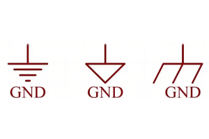
What is GND in the circuit?
on January 1th 2937
-
RJ-45 Connector Guide: RJ-45 Connector Color Codes, Wiring Schemes, R-J45 Applications, RJ-45 Datasheets
on January 1th 2499
-

Fiber Connector Types: SC Vs LC And LC Vs MTP
on January 1th 2089
-
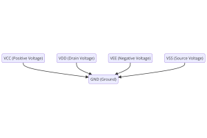
Understanding Power Supply Voltages in Electronics VCC, VDD, VEE, VSS, and GND
on November 9th 1890
-

Comparison Between DB9 and RS232
on January 1th 1761
-

What Is An LR44 Battery?
Electricity, that ubiquitous force, quietly permeates every aspect of our daily lives, from trivial gadgets to life-threatening medical equipment, it plays a silent role. However, truly grasping this energy, especially how to store and efficiently output it, is no easy task. It is against this background that this article will focus on a type of coin cell battery that may seem insignificant on the...on January 1th 1712
-
Understanding the Fundamentals:Inductance Resistance, andCapacitance
In the intricate dance of electrical engineering, a trio of fundamental elements takes center stage: inductance, resistance, and capacitance. Each bears unique traits that dictate the dynamic rhythms of electronic circuits. Here, we embark on a journey to decipher the complexities of these components, to uncover their distinct roles and practical uses within the vast electrical orchestra. Inductan...on January 1th 1652
-
CR2430 Battery Comprehensive Guide: Specifications, Applications and Comparison to CR2032 Batteries
What is CR2430 battery ?Benefits of CR2430 BatteriesNormCR2430 Battery ApplicationsCR2430 EquivalentCR2430 VS CR2032Battery CR2430 SizeWhat to look for when buying the CR2430 and equivalentsData Sheet PDFFrequently Asked Questions Batteries are the heart of small electronic devices. Among the many types available, coin cells play a crucial role, commonly found in calculators, remote controls, and ...on January 1th 1551
-
What Is RF and Why Do We Use It?
Radio Frequency (RF) technology is a key part of modern wireless communication, enabling data transmission over long distances without physical connections. This article delves into the basics of RF, explaining how electromagnetic radiation (EMR) makes RF communication possible. We will explore the principles of EMR, the creation and control of RF signals, and their wide-ranging uses. The article ...on January 1th 1538
-

CR2450 vs CR2032: Can The Battery Be Used Instead?
Lithium manganese batteries do have some similarities with other lithium batteries. High energy density and long service life are the characteristics they have in common. This kind of battery has won the trust and favor of many consumers because of its unique safety. Expensive tech gadgets? Small appliances in our homes? Look around and you'll see them everywhere. Among these many lithium-manganes...on January 1th 1511
HOT Part Number
-

08055C222KAT2A
AVX Corporation
CAP CER 2200PF 50V X7R 0805
SI8622BC-B-ISR
Skyworks Solutions Inc.
DGTL ISO 3750VRMS 2CH GP 8SOIC
SP705CN-L
MaxLinear, Inc.
IC SUPERVISOR 1 CHANNEL 8SOIC
MAX1967EUB-T
Analog Devices Inc./Maxim Integrated
PWM STEP-DOWN CONTROLLER
151033BS03000
Würth Elektronik
LED BLUE CLEAR 3MM ROUND T/H
FLT007A0-SRZ
ABB Power Electronics Inc.
LINE FILTER 75VDC 7A SMD
TPA4411MRTJRG4
Texas Instruments
IC AMP CLASS AB STER 100MW 20QFN
TLV2465IPW
Texas Instruments
IC OPAMP GP 4 CIRCUIT 16TSSOP
N1651QK220
IXYS
SCR 2.2KV 3253A WP2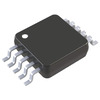
LT1945IMS#TRPBF
Analog Devices Inc.
IC REG BST SEPIC ADJ DL 10MSOP
LM2670SD-ADJ
Texas Instruments
IC REG BUCK ADJUSTABLE 3A 14VSON
THCV235
THine Solutions, Inc.
1LANE LVCMOS_V-BY-ONEHS 64QFN
CD54HC541F
Texas Instruments
CD54HC541 HIGH SPEED CMOS LOGIC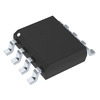
NCP1308DR2G
onsemi
IC OFFLINE SWITCH FLYBACK 8SOIC
GRM0335C1H4R4CD01D
Murata Electronics
CAP CER 4.4PF 50V C0G/NP0 0201
MP2188GQA-Z
Monolithic Power Systems Inc.
IC REG BUCK ADJ/FIX 3A DL 16QFN
C2012X5R2E152K085AA
TDK Corporation
CAP CER 1500PF 250V X5R 0805
STTA512FP
STMicroelectronics
DIODE GP 1.2KV 5A TO220FPAC -

LDB311G6005C-300
Murata Electronics
MULTI-LAY HYBRID BALUNS 1206
12065C822MAT2A
KYOCERA AVX
CAP CER 8200PF 50V X7R 1206
AD8350AR15-REEL7
Analog Devices Inc.
IC AMP DIFF LOW-DISTORTION 8SOIC
IL388T
Vishay Semiconductor Opto Division
OPTOISO 2.13KV 2CH TRANS 8SOP
STA310
STMicroelectronics
IC AUDIO DECODER 6+2CH 80-TQFP
MRF6S21050LSR3
NXP USA Inc.
FET RF 68V 2.16GHZ NI-400S
MBR16100CTG
onsemi
DIODE ARRAY SCHOTTKY 100V TO220
HCPL-7510-300E
Broadcom Limited
IC OPAMP ISOLATION 1 CIRC 8DIPGW
0505025.MXEP
Littelfuse Inc.
FUSE CERAMIC 25A 500VAC/VDC 3AB
IRF820ASPBF
Vishay Siliconix
MOSFET N-CH 500V 2.5A D2PAK
APTGF165DA60D1G
Microsemi Corporation
IGBT MODULE 600V 230A 730W D1
NP5Q128A13ESFC0E
Micron Technology Inc.
IC PCM 128MBIT SPI 66MHZ 16SO W
CRG0805F4K7
TE Connectivity Passive Product
RES SMD 4.7K OHM 1% 1/8W 0805
LC87F2932AVU-QIP-E
onsemi
MICROCONTROLLER 8-BIT LC8XX CPU
SMF24AT1G
Littelfuse Inc.
TVS DIODE 24VWM 38.9VC SOD123FL
RT0805BRE07182KL
YAGEO
RES SMD 182K OHM 0.1% 1/8W 0805
FSUSB23BQX
onsemi
IC USB SWITCH 2X2 16DQFN
NL17SZ02DFT2G
onsemi
IC GATE NOR 1CH 2-INP SC88A -
UUX1E101MNL1GS
Nichicon
CAP ALUM 100UF 20% 25V SMD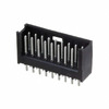
280509-1
TE Connectivity AMP Connectors
CONN HEADER VERT 18POS 2.54MM
NCP1247DD065R2G
onsemi
IC OFFLINE SWITCH FLYBACK 7SOIC
DAC667KP
Texas Instruments
DAC, PARALLEL, WORD INPUT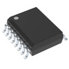
UCC12050DVE
Texas Instruments
DC DC CONVERTER 3.3V 5V 500MW
DMT6015LSS-13
Diodes Incorporated
MOSFET N-CH 60V 9.2A 8SO
CC0201KRX7R8BB821
YAGEO
CAP CER 820PF 25V X7R 0201
FSA2357BQX
onsemi
IC SWITCH DP3T 14DQFN
LFCN-3400D+
Mini-Circuits
LTCC LOW PASS FILTER, DC - 3400
MB9AF005PMC-G-SNE2
Infineon Technologies
IC MCU 32BIT FLASH 100LQFP
LTC2482IDD#PBF
Analog Devices Inc.
IC ADC 16BIT SIGMA-DELTA 10DFN
DSPIC30F4011-20I/PT
Microchip Technology
IC MCU 16BIT 48KB FLASH 44TQFP
MC100EP101MNR4G
onsemi
IC GATE OR/NOR QUAD 4INP 32-QFN
CD4516BCN
onsemi
IC BINARY COUNTER
ATSAMD21G16L-MNT
Microchip Technology
IC MCU 32BIT 64KB FLASH 48QFN
0805PC192KAT1A
KYOCERA AVX
CAP CER 1900PF 250V X7R 0805
SPM5012T-6R8M-LR
TDK Corporation
FIXED IND 6.8UH 1.6A 253MOHM SMD
TC51N3002ECBTR
Microchip Technology
IC SUPERVISOR 1 CHANNEL SOT23A-3