An In-Depth Look at the CC2530F128RHAT RF SoC: Features and Applications
Catalog
Overview of CC2530F128RHAT
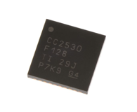
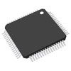
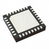
The CC2530F128RHAT stands as a notable radio frequency system-on-chip (RF SoC) produced by Texas Instruments. Falling under the RF System on a Chip - SoC classification, it epitomizes efficiency and compactness, encapsulated within a VQFN-40 package and employing SMD or SMT methodology. Operating at a frequency of 2.4 GHz, this chip exhibits versatility with a supply voltage range spanning from 2V to 3.6V, catering to diverse power requirements. With an 8-bit data bus width, it delivers swift and precise data processing capabilities. Crucially, to ensure optimal functionality, it operates within a wide temperature range of -40°C to 125°C, showingcasing resilience across varied environmental conditions. Furthermore, its feature set includes 4 timers, 8 ADC channels, and an impressive array of 21 I/O pins, underscoring its adaptability and applicability across a spectrum of electronic applications.
Alternative models:
• CC2530F32RHAT
Concrete applications of CC2530F128RHAT
• Health care
• Consumer electronics
• ZigBee systems (256-KB Flash)
• Lighting systems
• Industrial control and monitoring
• 2.4-GHz IEEE 802.15.4 systems
• Home/building automation
• Low-power wireless sensor networks
• RF4CE remote control systems (64-KB Flash and higher)
Advantages of CC2530F128RHAT
Hardware encryption engine
The integration of the hardware encryption engine enables the CC2530F128RHAT to perform encryption and decryption operations in real time during data processing, ensuring that sensitive data will not be intercepted or tampered with by unauthorized third parties during transmission. This real-time encryption mechanism greatly improves data confidentiality and effectively prevents the risk of data leakage.
Rich peripheral interfaces
The CC2530F128RHAT has a variety of general-purpose IO pins and serial interfaces, enabling it to be easily connected to a variety of external devices and sensors, improving system flexibility and scalability.
Powerful processing capability
The CC2530F128RHAT integrates a powerful 8-bit microcontroller with 8KB of RAM and 128KB of Flash memory, capable of handling complex communication protocol stacks and user applications.
High integration
In traditional system design, wireless communication modules and microcontrollers usually need to be selected, configured and connected separately, which not only increases the complexity of the system, but also may lead to signal interference, stability degradation and other problems. The integrated design of CC2530F128RHAT, on the other hand, integrates these two key components, making the whole system more efficient.
How to choose the energy-saving working mode for CC2530F128RHAT?
CC2530F128RHAT supports multiple working modes to meet the power consumption requirements in different application scenarios. To reduce power consumption, we need to choose an appropriate working mode based on the characteristics of the application. The following are the main operating modes and characteristics of the CC2530F128RHAT device:
Idle mode
In this mode, the microcontroller stops executing program code, but the RF transceiver can still work. The power consumption in this mode is lower and is suitable for application scenarios where system power consumption needs to be reduced but data still needs to be received.
Deep-sleep mode
In this mode, both the microcontroller and the RF transceiver stop working and can only be woken up by a reset signal. This mode's power consumption reaches the lowest level, so it is particularly suitable for scenarios where extremely low power consumption needs to be maintained for a long time.
Active mode
In this mode, the microcontroller and RF transceiver are both in normal working condition and can execute program code and process data. The power consumption in this mode is relatively high.
Power-down mode
In this mode, the microcontroller and RF transceiver stop working, but can be awakened by external interrupts. The power consumption in this mode is very low and is suitable for applications that require low power consumption for a long time.
To choose the appropriate working mode to reduce power consumption, we need to consider the following points:
Wake-up source
Depending on the wake-up source, we can choose power-down mode or deep sleep mode. If the wake-up source is an external interrupt, power-down mode can be selected; if the wake-up source is a reset signal, deep sleep mode can be selected.
4.6 Data transmission requirements
If the application requires frequent data transmission, we may need to select active mode. If data transmission is infrequent, we can choose idle mode or power-down mode to wake up the device when data needs to be transmitted.
Application requirements for real-time performance
If the application needs to process data or respond to events in real time, we may need to choose active mode or idle mode. In this case, we can consider configuring the RF transceiver in low-power mode in idle mode to reduce power consumption.
Technical parameters of CC2530F128RHAT
• Manufacturer: Texas Instruments
• Package / Case: VQFN-40
• Packaging: Tape & Reel (TR)
• Output Power: 4.5 dBm
• Data Bus Width: 8 bit
• ADC Resolution: 12 bit
• Supply Voltage: 2V ~ 3.6V
• Operating Frequency: 2.4 GHz
• Operating Temperature: -40°C ~ 125°C
• Program Memory Size: 128 kB
• Program Memory Type: Flash
• Number of ADC Channels: 8
• Number of I/Os: 21
• Number of Timers: 4 Timers
• Mounting Style: SMD/SMT
• Product Category: RF System on a Chip - SoC
Block diagram and architecture of CC2530F128RHAT
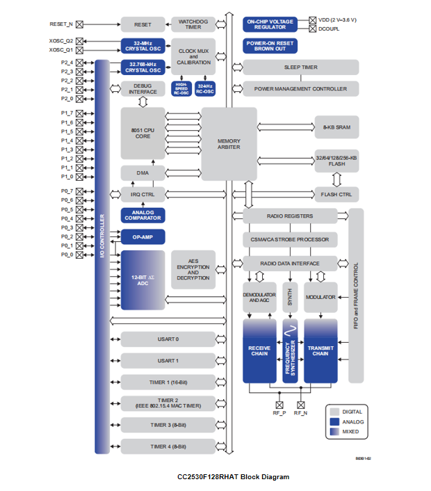
A block diagram of the CC2530F128RHAT is shown in the following figure. The modules can be roughly divided into one of three categories: CPU- and memory-related modules; modules related to peripherals, clocks, and power management; and radio-related modules. In the following subsections, a short description of each module that appears in the figure.
CPU and memory
The 8051 CPU core used in CC2530F128RHAT is a single-cycle 8051-compatible core. It has three different memory-access buses (SFR, DATA and CODE/XDATA) with single-cycle access to SFR, DATA, and the main SRAM. It also includes a debug interface and an 18-input extended interrupt unit.
The 8-KB SRAM maps to the DATA memory space and to parts of the XDATA memory spaces. The 8-KB SRAM is an ultralow-power SRAM that retains its contents even when the digital part is powered off (power modes 2 and 3). This is an important feature for low-power applications.
The 32/64/128/256 KB flash block provides in-circuit programmable non-volatile program memory for the device, and maps into the CODE and XDATA memory spaces. In addition to holding program code and constants, the non- volatile memory allows the application to save data that must be preserved such that it is available after restarting the device. Using this feature one can, e.g., use saved network-specific data to avoid the need for a full start-up and network find- and-join process.
The memory arbiter is at the heart of the system, as it connects the CPU and DMA controller with the physical memories and all peripherals through the SFR bus. The memory arbiter has four memory access points, access of which can map to one of three physical memories: an 8-KB SRAM, flash memory, and XREG/SFR registers. It is responsible for performing arbitration and sequencing between simultaneous memory accesses to the same physical memory.
The interrupt controller services a total of 18 interrupt sources, divided into six interrupt groups, each of which is associated with one of four interrupt priorities. Any interrupt service request is serviced also when the device is in idle mode by going back to active mode. Some interrupts can also wake up the device from sleep mode (power modes 1 to 3).
Peripherals
The CC2530F128RHAT includes many different peripherals that allow the application designer to develop advanced applications. First, the CC2530F128RHAT has multiple serial communication interfaces that allow efficient and reliable data transmission between the chip and external devices. These interfaces usually include USART (Universal Synchronous Asynchronous Receiver Transmitter), etc., which support multiple communication protocols, allowing the chip to seamlessly connect with various types of devices. Secondly, CC2530F128RHAT is also equipped with ADC. ADC is a circuit that converts analog signals into digital signals, which enables the chip to process data from analog sensors. This conversion is critical for many applications because it allows the chip to accurately analyze and process analog signals. In addition, GPIO (General Purpose Input/Output) pins are an important channel for the chip to interact with the outside world. CC2530F128RHAT provides multiple GPIO pins that can be configured in input or output mode for reading the status of external devices or controlling the operation of external devices. Through GPIO pins, the chip can interact with other hardware components, sensors or actuators to implement various complex functions. In addition to the peripherals mentioned above, the CC2530F128RHAT may also include other peripherals, such as battery monitors, temperature sensors, etc. The battery monitor is used to monitor the voltage and status of the battery in real time to ensure that the chip can take appropriate measures when the battery power is low. The temperature sensor is used to detect the temperature of the chip or the surrounding environment.
Clocks and power management
The digital core and peripherals are powered by a 1.8-V low-dropout voltage regulator. It provides power management functionality that enables low power operation for long battery life using different power modes. Five different reset sources exist to reset the device.
How to improve the reliability and stability of CC2530F128RHAT?
To improve the reliability and stability of CC2530F128RHAT, we can consider the following aspects:
Wireless communication optimization
Data verification: We can use data verification mechanisms (such as CRC) to ensure data integrity.
Signal quality: We need to ensure good signal quality in the wireless communication environment to avoid interference and conflicts.
Protocol selection: we select appropriate wireless communication protocols and parameter settings to adapt to the application requirements and communication environment.
Environmental adaptation
Humidity and vibration: We should consider factors such as humidity and vibration in the application environment and take appropriate measures to protect the equipment.
Temperature range: We should make sure that the CC2530F128RHAT works within its recommended temperature range to avoid the effects of extreme temperatures on the device.
Hardware design
Antenna matching: We need to make sure that the antenna matches the RF interface of the CC2530F128RHAT to get the best wireless communication performance.
Power stability: We use a stable power supply and use appropriate filtering and decoupling capacitors to reduce power noise.
Peripheral circuit design: We should design the peripheral circuits properly, such as impedance matching and filters, to minimize electromagnetic interference (EMI) and electromagnetic compatibility (EMC) problems.
Firmware optimization
Low-power design: We have to optimize the code to reduce power consumption, extend the running time of the device, and reduce errors that may be caused by power fluctuations.
Software watchdog: We need to implement a software watchdog to detect and recover from potential software failures and prevent the program from running away.
Error handling: We implement appropriate error detection and handling mechanisms in the code, including the detection and handling of hardware errors, communication errors, data checksums, etc.
Frequently Asked Questions [FAQ]
1. What is an RF SoC?
It is a system-on-chip (SoC) for communications that contains multiple radio frequency (RF) components.
2. What is the replacement and equivalent of CC2530F128RHAT?
You can replace the CC2530F128RHAT with CC2530F256RHAR, CC2530F256RHAT, or CC2530F32RHAT.
3. Can the CC2530F128RHAT be programmed and customized?
Yes, the CC2530F128RHAT can be programmed using standard development tools such as TI's Code Composer Studio or IAR Embedded Workbench. Additionally, it supports Over-the-Air (OTA) firmware updates, allowing for remote programming and customization.
About us
ALLELCO LIMITED
Read more
Quick inquiry
Please send an inquiry, we will respond immediately.
Explore the STM32F103RET6 Microcontroller: Features, Uses, and Programming Insights
on August 30th
Comprehensive Analysis of the TPS82085SILR: Features, Thermal Considerations, and Use Cases
on August 30th
Popular Posts
-

What is GND in the circuit?
on January 1th 3036
-

RJ-45 Connector Guide: RJ-45 Connector Color Codes, Wiring Schemes, R-J45 Applications, RJ-45 Datasheets
on January 1th 2608
-

Fiber Connector Types: SC Vs LC And LC Vs MTP
on January 1th 2162
-
Understanding Power Supply Voltages in Electronics VCC, VDD, VEE, VSS, and GND
on November 13th 2067
-

Comparison Between DB9 and RS232
on January 1th 1789
-

What Is An LR44 Battery?
Electricity, that ubiquitous force, quietly permeates every aspect of our daily lives, from trivial gadgets to life-threatening medical equipment, it plays a silent role. However, truly grasping this energy, especially how to store and efficiently output it, is no easy task. It is against this background that this article will focus on a type of coin cell battery that may seem insignificant on the...on January 1th 1754
-
Understanding the Fundamentals:Inductance Resistance, andCapacitance
In the intricate dance of electrical engineering, a trio of fundamental elements takes center stage: inductance, resistance, and capacitance. Each bears unique traits that dictate the dynamic rhythms of electronic circuits. Here, we embark on a journey to decipher the complexities of these components, to uncover their distinct roles and practical uses within the vast electrical orchestra. Inductan...on January 1th 1704
-

CR2430 Battery Comprehensive Guide: Specifications, Applications and Comparison to CR2032 Batteries
What is CR2430 battery ?Benefits of CR2430 BatteriesNormCR2430 Battery ApplicationsCR2430 EquivalentCR2430 VS CR2032Battery CR2430 SizeWhat to look for when buying the CR2430 and equivalentsData Sheet PDFFrequently Asked Questions Batteries are the heart of small electronic devices. Among the many types available, coin cells play a crucial role, commonly found in calculators, remote controls, and ...on January 1th 1640
-

What Is RF and Why Do We Use It?
Radio Frequency (RF) technology is a key part of modern wireless communication, enabling data transmission over long distances without physical connections. This article delves into the basics of RF, explaining how electromagnetic radiation (EMR) makes RF communication possible. We will explore the principles of EMR, the creation and control of RF signals, and their wide-ranging uses. The article ...on January 1th 1620
-
Comprehensive guide to hFE in transistors
Transistors are crucial components in modern electronic devices, enabling signal amplification and control. This article delves into the knowledge surrounding hFE, including how to select a transistor's hFE value, how to find hFE, and the gain of different types of transistors. Through our exploration of hFE, we gain a deeper understanding of how transistors work and their role in electronic circu...on November 13th 1562

