USB3300 Transceiver: Datasheet, Pinout, and Specifications
The USB3300 stands as a high-performance USB transceiver engineered to maintain exceptional stability and functionality across diverse thermal environments. Central to modern electronic designs, it offers a detailed exploration of its capabilities, pin specifications, and technical parameters, empowering designers to fully leverage its potential in a variety of applications. This article delves into the intricacies of the USB3300, showcasing its importance in enhancing connectivity and performance in electronics today.Catalog
What is the USB3300?
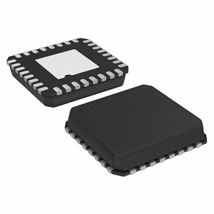
The USB3300 transceiver is an important part for handling high-speed USB connections and can work well in extreme temperatures. It uses a low-pin ULPI interface, which makes it easy to connect with other ULPI-compatible devices. This new design reduces the number of pins needed, from 54 in the older UTMI+ interface down to just 12. This improvement means there’s no need for complicated UTMI-to-ULPI adapters, allowing for faster data transfers with less delay. The USB3300 also supports different modes, device, host, and OTG (On-The-Go) which gives more flexibility to add host or OTG features as they build their products. The USB3300 can easily switch between device, host, and OTG modes, making it a versatile option for a wide range of uses, from simple USB accessories to complex host systems. This flexibility allows to build USB systems that can change roles depending on the need, which is increasingly useful for modern electronics. Components that can adapt in this way tend to last longer in the market compared to less flexible alternatives. With Microchip’s advanced technology in a compact package, adding high-speed USB to new designs is simpler and faster. The USB3300 requires few extra components and has built-in termination resistors, which further eases integration. By focusing on simplicity and high integration, you can spend more time on innovation rather than managing complex components. This streamlined approach speeds up development, reduces design errors, and improves product reliability, helping products succeed in the marketplace.
USB3300 Pin Configuration
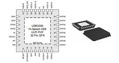
|
Pin No |
Pin Name |
Description |
|
1 |
GND |
Ground |
|
2 |
GND |
Ground |
|
3 |
CPEN |
External 5 volt supply enable. This pin is used to enable
the external Vbus power supply. The CPEN pin is low on POR. |
|
4 |
VBUS |
VBUS pin of the USB cable. The USB3300 uses this pin for
the Vbus comparator inputs and for Vbus pulsing during session request
protocol. |
|
5 |
ID |
ID pin of the USB cable. For non-OTG applications this
pin can be floated. For an A-Device ID = 0. For a B-Device ID = 1. |
|
6 |
VDD3.3 |
3.3V Supply. A 0.1uF bypass capacitor should be connected
between this pin and the ground plane on the PCB. |
|
7 |
DP |
D+ pin of the USB cable. |
|
8 |
DM |
D- pin of the USB cable. |
|
9 |
RESET |
Optional active high transceiver reset. This is the same
as a write to the ULPI Reset, address 04h, bit 5. This does not reset the
ULPI register set. This pin includes an integrated pull-down resistor to
ground. If not used, this pin can be floated or connected to ground
(recommended). |
|
10 |
EXTVBUS |
External Vbus Detect. Connect to fault output of an
external USB power switch or an external Vbus Valid comparator. This pin has
a pull down resistor to prevent it from floating when the ULPI bit
UseExternalVbusIndicator is set to 0. |
|
11 |
NXT |
The PHY asserts NXT to throttle the data. When the Link
is sending data to the PHY, NXT indicates when the current byte has been
accepted by the PHY. The Link places the next byte on the data bus in the
following clock cycle. |
|
12 |
DIR |
Controls the direction of the data bus. When the PHY has
data to transfer to the Link, it drives DIR high to take ownership of the
bus. When the PHY has no data to transfer it drives DIR low and monitors the
bus for commands from the Link. The PHY will pull DIR high whenever the
interface cannot accept data from the Link, such as during PLL start-up. |
|
13 |
STP |
The Link asserts STP for one clock cycle to stop the data
stream currently on the bus. If the Link is sending data to the PHY, STP
indicates the last byte of data was on the bus in the previous cycle. |
|
14 |
CLKOUT |
60MHz reference clock output. All ULPI signals are driven
synchronous to the rising edge of this clock. |
|
15 |
VDD1.8 |
1.8V for digital circuitry on chip. Supplied by On-Chip
Regulator when REG_EN is active. Place a 0.1uF capacitor near this pin and
connect the capacitor from this pin to ground. Connect pin 15 to pin 26. |
|
16 |
VDD3.3 |
A 0.1uF bypass capacitor should be connected between this
pin and the ground plane on the PCB. |
|
17 |
DATA[7] |
8-bit bi-directional data bus. Bus ownership is
determined by DIR. The Link and PHY initiate data transfers by driving a
non-zero pattern onto the data bus. ULPI defines interface timing for a
single-edge data transfers with respect to rising edge of CLKOUT. DATA[7] is
the MSB and DATA[0] is the LSB. |
|
18 |
DATA[6] |
|
|
19 |
DATA[5] |
|
|
20 |
DATA[4] |
|
|
21 |
DATA[3] |
|
|
22 |
DATA[2] |
|
|
23 |
DATA[1] |
|
|
24 |
DATA[0] |
|
|
25 |
VDD3.3 |
A 0.1uF bypass capacitor should be connected between this
pin and the ground plane on the PCB. |
|
26 |
VDD1.8 |
1.8V for digital circuitry on chip. Supplied by On-Chip
Regulator when REG_EN is active. When using the internal regulators, place a
4.7uF low-ESR capacitor near this pin and connect the capacitor from this pin
to ground. Connect pin 26 to pin 15. Do not connect VDD1.8 to VDDA1.8 when
using internal regulators. When the regulators are disabled, pin 29 may be
connected to pins 26 and 15. |
|
27 |
XO |
Crystal pin. If using an external clock on XI this pin
should be floated. |
|
28 |
XI |
Crystal pin. A 24MHz crystal is supported. The crystal is
placed across XI and XO. An external 24MHz clock source may be driven into XI
in place of a crystal. |
|
29 |
VDDA1.8 |
1.8V for analog circuitry on chip. Supplied by On-Chip
Regulator when REG_EN is active. Place a 0.1uF capacitor near this pin and
connect the capacitor from this pin to ground. When using the internal
regulators, place a 4.7uF low-ESR capacitor near this pin in parallel with
the 0.1uF capacitor. Do not connect VDD1.8A to VDD1.8 when using internal
regulators. When the regulators are disabled, pin 29 may be connected to pins
26 and 15. |
|
30 |
VDD3.3 |
Analog 3.3 volt supply. A 0.1uF low ESR bypass capacitor
connected to the ground plane of the PCB is recommended. |
|
31 |
REG_EN |
On-Chip 1.8V regulator enable. Connect to ground to
disable both of the on chip (VDDA1.8 and VDD1.8) regulators. When regulators
are disabled: • External 1.8V must be supplied to VDDA1.8 and VDD1.8 pins.
When the regulators are disabled, VDDA1.8 may be connected to VDD1.8 and a
bypass capacitor (0.1uF recommended) should be connected to each pin. • The
voltage at VDD3.3 must be at least 2.64V (0.8 * 3.3V) before voltage is
applied to VDDA1.8 and VDD1.8. |
|
32 |
RBIAS |
External 12KΩ +/- 1% bias resistor to ground. |
USB3300 Symbol, Footprint, and CAD Model
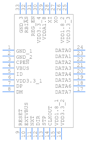
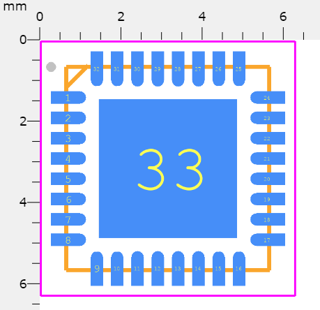
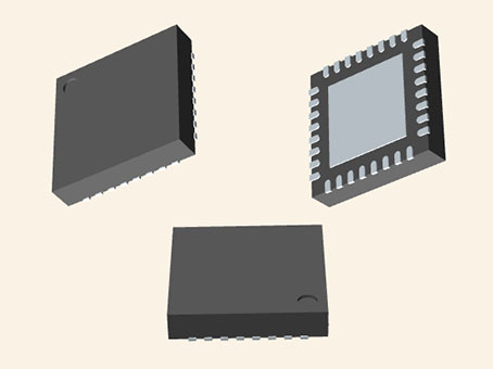
Features of the USB3300
Certification and Compliance
The USB3300 transceiver stands out with its USB-IF certification, highlighting its conformity to Hi-Speed under USB 2.0 standards. Its alignment with the ULPI Specification 1.1 in 8-bit mode reinforces its technical solidity, facilitating broad interoperability across various USB systems.
Energy Efficiency Considerations
A distinctive feature is its low operational currents, which enhance energy management in both bus-powered and battery-dependent devices. This makes it compatible with applications necessitating minimal power usage while delivering necessary performance.
Protection and Connectivity
The transceiver extends remarkable electrostatic discharge (ESD) protection, a factor in safeguarding against potential damage. The inclusion of integrated characteristics supporting On-the-Go (OTG) applications broadens its applicability. It allows for fluid connection between multiple devices independently of a host computer, reflecting the evolving trends in device connectivity.
Adaptability and Versatility
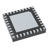
Designed to function reliably within an industrial temperature spectrum, the USB3300 stands as a dependable option for environments subject to varying and at times severe conditions. Its compact 5x5mm QFN package boosts its adaptability, enabling seamless integration into space-restrictive designs without sacrificing functionality. This fosters efficient design configurations and potentially sparks innovations in product dimensions and shape.
USB3300 Technical Specifications
Technical specifications, characteristics, parameters, and similar components to the Microchip Technology USB3300-EZK.
|
Type |
Parameter |
|
Factory Lead Time |
11 Weeks |
|
Mount |
Surface Mount |
|
Number of Pins |
32 |
|
Usage Level |
Industrial grade |
|
Packaging |
Tray |
|
JESD-609 Code |
e3 |
|
Part Status |
Active |
|
Number of Terminations |
32 |
|
Terminal Position |
QUAD |
|
Supply Voltage |
3.3V |
|
Base Part Number |
USB3300 |
|
Voltage |
5V |
|
Operating Supply Current |
54.7mA |
|
Data Rate |
480 Mbps |
|
Contact Plating |
Tin |
|
Package / Case |
32-VQFN Exposed Pad |
|
Weight |
188.609377mg |
|
Operating Temperature |
-40°C~85°C |
|
Published |
2005 |
|
Pbfree Code |
yes |
|
Moisture Sensitivity Level (MSL) |
3 (168 Hours) |
|
Voltage - Supply |
3V~3.6V |
|
Peak Reflow Temperature (Cel) |
260 |
|
Time@Peak Reflow Temperature-Max (s) |
40 |
|
Function |
Controller |
|
Interface |
ULPI |
|
Number of Ports |
1 |
|
Protocol |
USB |
|
Telecom IC Type |
INTERFACE CIRCUIT |
|
USB |
USB 2.0 |
|
Ambient Temperature Range High |
85°C |
|
Length |
5mm |
|
REACH SVHC |
No SVHC |
|
RoHS Status |
ROHS3 Compliant |
|
ESD Protection |
Yes |
|
Standards |
USB 2.0, OTG |
|
Height |
1mm |
|
Width |
5mm |
|
Radiation Hardening |
No |
|
Lead Free |
Lead Free |
Alternatives of the USB3300
|
Part
Number |
Manufacturer |
Package / Case |
Number of Pins |
Interface |
Number of Ports |
Data Rate |
Supply Voltage |
RoHS Status |
Mount |
|
USB3300-EZK |
Microchip Technology |
32-VFQFN Exposed Pad |
32 |
ULPI |
1 |
480 Mbps |
3.3 V |
ROHS3 Compliant |
Surface Mount |
|
78Q2123/F |
Maxim Integrated |
24-VFQFN Exposed Pad |
24 |
UART, USB |
1 |
480 Mbps |
1.8 V |
ROHS3 Compliant |
Surface Mount |
|
USB3343-CP |
Microchip Technology |
28-VFQFN Exposed Pad |
28 |
- |
2 |
480 Mbps |
3.3 V |
ROHS3 Compliant |
Surface Mount |
|
USB2412-DZK |
Microchip Technology |
32-VFQFN Exposed Pad |
32 |
- |
- |
100 Mbps |
3.3 V |
ROHS3 Compliant |
Surface Mount |
|
USB2422-I/MJ |
Microchip Technology |
24-VFQFN Exposed Pad |
24 |
- |
- |
480 Mbps |
3.3 V |
ROHS3 Compliant |
Surface Mount |
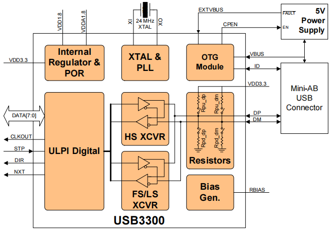
Functional Block Diagram of the USB3300
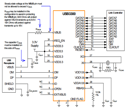
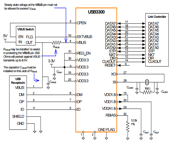
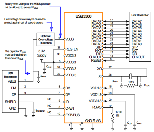
Application Diagrams of the USB3300
Applications of the USB3300
Expanding Device Integration
The USB3300 is at the heart of countless devices, deftly bridging consumer electronics with industrial applications. When integrated into mobile phones and PDAs, its contribution transcends mere connectivity. It boosts data transfer efficiency, enabling seamless synchronization with a multitude of digital platforms. In a rapidly evolving world that feeds on real-time data exchange, this efficiency allows to interact more fluidly with their devices.
Advancing Media Solutions
Within media players, the USB3300 enabling swift transfer and playback of high-fidelity media files. As media content becomes increasingly intricate and voluminous, robust data solutions become important . Implementing such components underlines an industry shift towards minimizing latency.
Industrial Optimization
For industrial purposes, incorporating the USB3300 into scanners signifies a step towards streamlined operational workflows. Its ability to process large data volumes efficiently and reliably thrives in environments demanding accuracy.
Balancing Performance and Practicality
The balance of performance and practicality is vividly illustrated by the USB3300's extensive versatility across diverse domains. It mirrors a broader movement toward crafting technology that excels in performance while being seamlessly integrable into existing systems. This adaptability is appreciated by many who seek to upgrade or expand their technological infrastructure with ease.
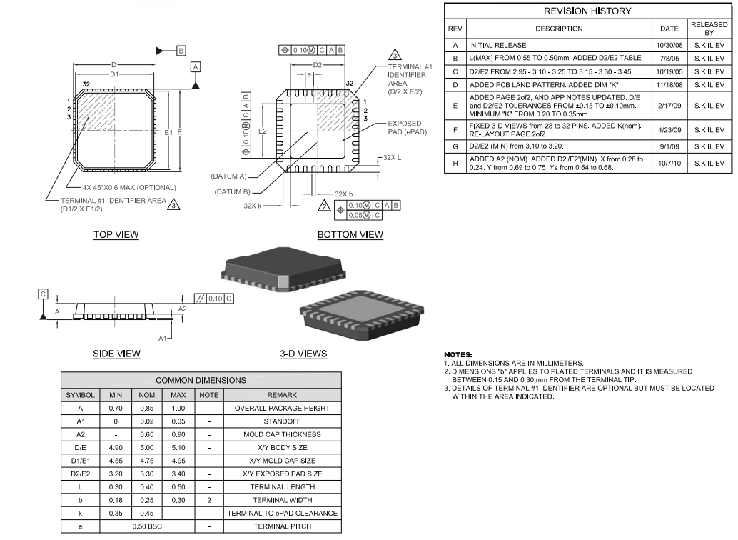
Package for USB3300
USB3300 Manufacturer Information
Located in Arizona, Microchip Technology excels in creating intelligent embedded control solutions. From its early days, the company has played a transformative role, enhancing design efficiency and aiding various sectors in speeding up their time-to-market. Recognized for its innovation, the USB3300 is a prominent element in Microchip's diverse portfolio, reflecting a commitment to technical achievement. The USB3300 signifies a remarkable progression in embedded system design, catering to numerous applications, performance and efficiency. Advances in technology have honed its practical application, integrating effectively into complex designs that require quick data transfer and stable connections. Though some argue that reliance on such components might complicate system integration, the notable advantages far outweigh these concerns. Microchip Technology's trajectory showcases an astute grasp of market needs and the vision to anticipate tech trends, positioning the company as a harbinger of future innovations.
Datasheet PDF
USB3300-EZK Datasheets:
Label and Packing Changes 23/Sep/2015.pdf
MBB/Label Chgs 16/Nov/2018.pdf
SCC Site Qualification 20/Apr/2015.pdf
78Q2123/F Datasheets:
Maxim Integrated RoHS Cert.pdf
Material Declaration 78Q2123/F.pdf
USB3343-CP Datasheets:
Label and Packing Changes 23/Sep/2015.pdf
MBB/Label Chgs 16/Nov/2018.pdf
USB2412-DZK Datasheets:
USB2422-I/MJ Datasheets:
Cylindrical Battery Holders.pdf
Label and Packing Changes 23/Sep/2015.pdf
MBB/Label Chgs 16/Nov/2018.pdf
About us
ALLELCO LIMITED
Read more
Quick inquiry
Please send an inquiry, we will respond immediately.
Frequently Asked Questions [FAQ]
1. What roles does the USB3300 fulfill?
It functions as a USB Physical Layer Transceiver, enabling high-speed data transfers. The USB3300 excels at facilitating seamless communication within intricate electronic ecosystems, akin to the meticulous coordination required in large-scale human endeavors.
2. How does USB3300 interact with ULPI-compliant layers?
It interfaces via a low pin count setup, which brings enhanced simplicity and reliability. This mirrors the effectiveness of a streamlined protocol in simplifying complex operations across diverse sectors.
3. How does the pin layout of ULPI differ from UTMI+?
By reducing the 54-pin UTMI+ interface to just 12 pins, it optimizes space and decreases complexity. This reflects a practice seen in industries where minimizing resources can still yield high-quality outputs.
4. What core philosophy is reflected in the design approach of USB3300?
The design strategically incorporates ULPI, reducing dependency on additional wrappers. This approach mirrors the idea that cutting down on extra components leads to more robust and cost-effective solutions, much like strategic resource management in projects.
5. What benefits in terms of latency does USB3300 offer?
The USB3300 delivers reduced latency for both data transmission and reception, for use cases requiring swift response. This is comparable to how rapid information processing is valued in decision-making processes.
6. Are additional pins needed for host/OTG functionality with USB3300?
No extra pins are required, aligning with the principle of maintaining efficiency while avoiding unnecessary complexity, akin to well-designed systems across various disciplines.
7. How is Hi-Speed USB integration facilitated by USB3300?
The integration is facilitated through its built-in ULPI interface and requires minimal extra components. This design philosophy emphasizes simplicity, promoting durability and ease, principles cherished in product lifecycle management.
8. What are the size dimensions of the USB3300?
Its compact size, measuring 5mm by 5mm, underscores a technological trend where miniaturization complements functionality without compromise. This mirrors consumer electronics where devices grow smaller yet sustain performance.
9. Which termination resistors are embedded in USB3300?
It includes built-in DP and DM termination resistors. This integration enhances reliability and simplifies design, resonating with engineering philosophies that support built-in efficiencies to better system integrity.
BNO055 Orientation Sensor: Architecture, Pinout, and Datasheet
on November 12th
1N4148 Signal Diode: Datasheet, Pinout, and Equivalents
on November 12th
Popular Posts
-
What is GND in the circuit?
on January 1th 3162
-

RJ-45 Connector Guide: RJ-45 Connector Color Codes, Wiring Schemes, R-J45 Applications, RJ-45 Datasheets
on January 1th 2737
-
Understanding Power Supply Voltages in Electronics VCC, VDD, VEE, VSS, and GND
on November 17th 2353
-

Fiber Connector Types: SC Vs LC And LC Vs MTP
on January 1th 2214
-

Comparison Between DB9 and RS232
on January 1th 1833
-

What Is An LR44 Battery?
Electricity, that ubiquitous force, quietly permeates every aspect of our daily lives, from trivial gadgets to life-threatening medical equipment, it plays a silent role. However, truly grasping this energy, especially how to store and efficiently output it, is no easy task. It is against this background that this article will focus on a type of coin cell battery that may seem insignificant on the...on January 1th 1805
-
Understanding the Fundamentals:Inductance Resistance, andCapacitance
In the intricate dance of electrical engineering, a trio of fundamental elements takes center stage: inductance, resistance, and capacitance. Each bears unique traits that dictate the dynamic rhythms of electronic circuits. Here, we embark on a journey to decipher the complexities of these components, to uncover their distinct roles and practical uses within the vast electrical orchestra. Inductan...on January 1th 1759
-

CR2430 Battery Comprehensive Guide: Specifications, Applications and Comparison to CR2032 Batteries
What is CR2430 battery ?Benefits of CR2430 BatteriesNormCR2430 Battery ApplicationsCR2430 EquivalentCR2430 VS CR2032Battery CR2430 SizeWhat to look for when buying the CR2430 and equivalentsData Sheet PDFFrequently Asked Questions Batteries are the heart of small electronic devices. Among the many types available, coin cells play a crucial role, commonly found in calculators, remote controls, and ...on January 1th 1724
-
What Is RF and Why Do We Use It?
Radio Frequency (RF) technology is a key part of modern wireless communication, enabling data transmission over long distances without physical connections. This article delves into the basics of RF, explaining how electromagnetic radiation (EMR) makes RF communication possible. We will explore the principles of EMR, the creation and control of RF signals, and their wide-ranging uses. The article ...on January 1th 1713
-
Comprehensive guide to hFE in transistors
Transistors are crucial components in modern electronic devices, enabling signal amplification and control. This article delves into the knowledge surrounding hFE, including how to select a transistor's hFE value, how to find hFE, and the gain of different types of transistors. Through our exploration of hFE, we gain a deeper understanding of how transistors work and their role in electronic circu...on November 17th 1683


