TPS1H100BQPWPRQ1 High-Side Power Switch: Datasheet, Layout, and Pinout
This article delves into the technological intricacies and applications of the TPS1H100BQPWPRQ1, a high-side power switch developed by Texas Instruments. Noted for integrating an NMOS power FET with a charge pump, this device enhances power management efficiency for reliable performance in automotive and industrial applications. We will explore the switch’s design, pin configurations, and technical specifications to provide a deep understanding of its functional excellence and application versatility.Catalog
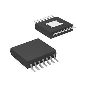
What is the TPS1H100BQPWPRQ1?
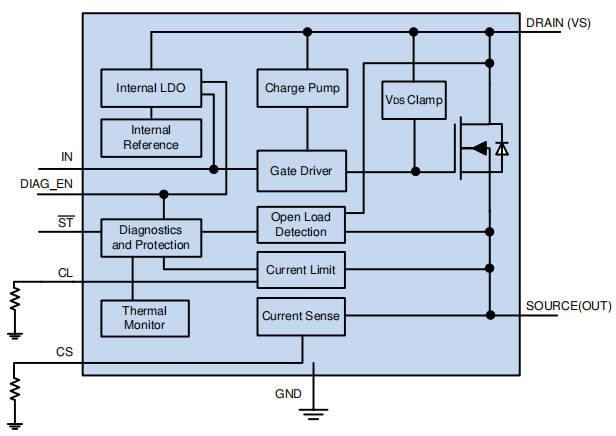
The TPS1H100BQPWPRQ1 is crafted to excel in power management applications, merging an NMOS power FET with a robust charge pump. Its performance is remarkable in single-channel operations, where superior protection features facilitate effective load management. The inclusion of advanced diagnostic and current-sense functionalities greatly enhances the reliability of the system. The device boasts an adaptable current-limit function, which contributes to its durability across a variety of demanding applications.
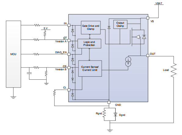
This device exemplifies remarkable versatility by enabling microcontroller interface multiplexing. It achieves this by switching diagnostics to a high-impedance mode when diagnostics are not in play. This kind of flexibility supports a more efficient and streamlined circuit design in practice. The TPS1H100BQPWPRQ1 is engineered to meet the diverse demands commonly encountered in different applications.
The variance between versions A and B reflects a considerate design that accommodates diverse user needs. Version A’s open-drain status reporting requires a pull-up to the microcontroller's supply, while version B enhances monitoring with current sensing capabilities. The K value remains constant and is resilient to environmental changes in the electronics field a reliable benchmark for predicting product performance across different conditions.
TPS1H100BQPWPRQ1 Pin Configuration
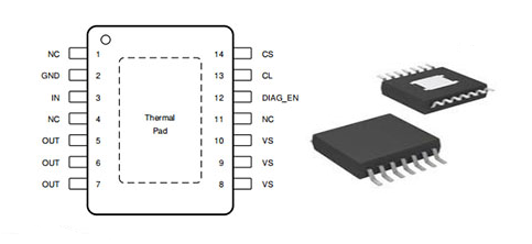
|
Pin Number |
Pin Name |
Description |
|
1 |
NC |
No connection; should be left unconnected |
|
2 |
GND |
Ground pin |
|
3 |
IN |
Input pin; used to control the device |
|
4 |
NC |
No connection; should be left unconnected |
|
5, 6, 7 |
OUT |
Output pins connected to the load (NMOS source) |
|
8, 9, 10 |
VS |
Supply voltage input from the battery |
|
11 |
NC |
No connection; should be left unconnected |
|
12 |
DIAG_EN |
Diagnostic enable pin; connects to MCU for
enabling/disabling diagnostics |
|
13 |
CL |
Current limit setting pin; configurable with an external
resistor |
|
14 |
CS |
Current sense output pin; provides feedback for load
current |
TPS1H100BQPWPRQ1 Symbol, Footprint, and CAD Model
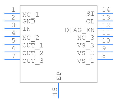
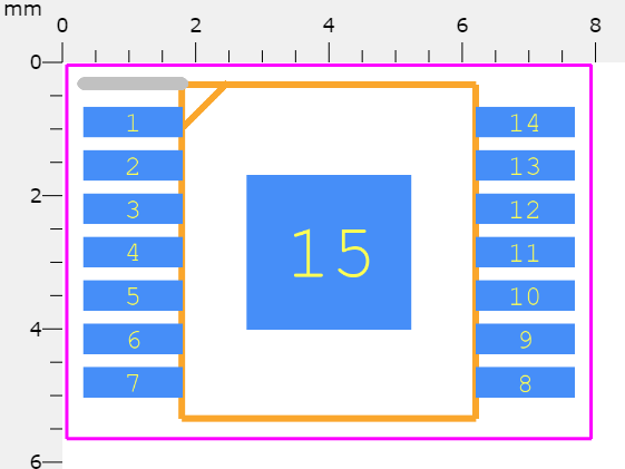
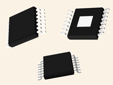
Features of the TPS1H100BQPWPRQ1
• Meets AEC-Q100 standards for dependability in harsh automotive environments.
• Supports functional safety, prioritizing reliability in automotive systems.
• Operates from 3.5V to 40V, covering diverse application needs.
• Reduces standby power to <0.5 µA, extending battery life and promoting energy efficiency.
• Functions reliably in extreme temperatures (-40°C to 150°C).
• Designed to handle intense heat and cold typical of engine compartments.
• Includes overload, short-circuit, and thermal shutdown protections to prevent damage during faults.
• Thermal shutdown shields the device in short-circuit scenarios.
• Provides accurate current monitoring.
• Adjustable current limits ensure flexibility across varied automotive circuits.
• Incorporates UVLO (Under Voltage Lock Out) and reverse battery protection to handle voltage inconsistencies.
• Ensures system stability in unpredictable automotive electrical environments.
• Features enhanced fault detection for output state supervision and thermal anomaly identification.
• Streamlined maintenance through actionable diagnostic insights.
• Housed in a 14-Pin Thermally-Enhanced PWP Package for effective heat dissipation.
• Maintains efficiency and reliability under high usage conditions.
TPS1H100BQPWPRQ1 Technical Specifications
|
Type |
Parameter |
|
Lifecycle Status |
ACTIVE (Last Updated: 6 days ago) |
|
Mounting Type |
Surface Mount |
|
Surface Mount |
YES |
|
Operating Temperature |
-40°C~125°C TA |
|
Series |
Automotive, AEC-Q100 |
|
Pbfree Code |
yes |
|
Moisture Sensitivity Level (MSL) |
3 (168 Hours) |
|
ECCN Code |
EAR99 |
|
Terminal Position |
DUAL |
|
Peak Reflow Temperature (Cel) |
260 |
|
Supply Voltage |
13.5V |
|
Base Part Number |
TPS1H100 |
|
Factory Lead Time |
8 Weeks |
|
Package / Case |
14-PowerTSSOP (0.173, 4.40mm Width) |
|
Number of Pins |
14 |
|
Packaging |
Tape & Reel (TR) |
|
JESD-609 Code |
e4 |
|
Part Status |
Active |
|
Number of Terminations |
14 |
|
Terminal Finish |
Nickel/Palladium/Gold (Ni/Pd/Au) |
|
Terminal Form |
GULL WING |
|
Number of Functions |
1 |
|
Time@Peak Reflow Temperature-Max (s) |
NOT SPECIFIED |
|
Number of Outputs |
1 |
|
Output Type |
N-Channel |
|
Supply Voltage-Max (Vsup) |
40V |
|
Interface |
On/Off |
|
Voltage - Supply (Vcc/Vdd) |
Not Required |
|
Switch Type |
General Purpose |
|
Voltage - Load |
5V~40V |
|
Turn On Time |
50 μs |
|
Rds On (Typ) |
80m Ω |
|
Turn Off Time |
50 μs |
|
Ambient Temperature Range High |
125°C |
|
Features |
Status Flag |
|
Length |
5mm |
|
Thickness |
1mm |
|
Lead Free |
Lead Free |
|
Max Output Current |
4A |
|
Supply Voltage-Min (Vsup) |
5V |
|
Output Configuration |
High Side |
|
Input Type |
Non-Inverting |
|
Ratio - Input |
1:01 |
|
Fault Protection |
Current Limiting (Adjustable), Open Load Detect, Over
Temperature, UVLO |
|
Output Peak Current Limit-Nom |
7A |
|
Max Junction Temperature (Tj) |
150°C |
|
Built-in Protections |
TRANSIENT: OVER CURRENT; THERMAL; UNDER VOLTAGE |
|
Output Current Flow Direction |
SINK |
|
Height |
1.2mm |
|
Width |
4.4mm |
|
RoHS Status |
ROHS3 Compliant |
Functional Block Diagram of TPS1H100BQPWPRQ1
Application Diagram for TPS1H100BQPWPRQ1
Layout of the TPS1H100BQPWPRQ1
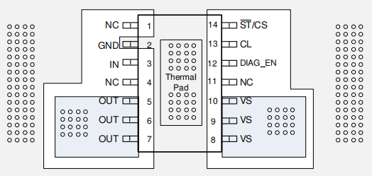
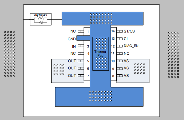
To prevent overheating, the device's temperature (TJ) must stay below 150°C, as high output currents can cause heat buildup. While the HTSSOP package handles heat well, effective PCB design for proper heat dissipation and device longevity. To improve heat transfer, maximize copper coverage on the PCB since copper efficiently carries heat away, especially when no additional heat sinks are present. Place as many thermal vias as possible under the package's ground pad to enhance thermal conductivity, and ensure all vias are fully plated or filled to avoid solder gaps. At least 85% of the ground pad should have solder coverage to maintain reliable performance.
Without a GND Network
If there’s no GND network on the PCB, connect the thermal pad directly to the board’s GND copper to improve heat dissipation. The picture below shows the pin configuration and layout of an electronic device, highlighting connections for ground, input, output, and various control functions, but without a ground network illustrated.
Layout Without a GND Network
With a GND Network
If a GND network is present, connect the thermal pad to the board’s GND copper using one trace through the GND network. The picture below shows the pin configuration and layout of an electronic device, featuring a detailed ground network and connections for power, inputs, outputs, and various control signals.
Layout With a GND Network
Applications of TPS1H100BQPWPRQ1
High-side Power Switching for Automotive Modules
High-side switching plays a role in automotive systems, facilitating the delivery of power to modules, including lighting systems, control units, and entertainment components. The TPS1H100BQPWPRQ1 excels in managing this power switching, which not only boosts efficiency but also enhances safety by reducing the likelihood of short circuits. As vehicles evolve with advanced electronic features, the necessity for robust, efficient, and compact power management solutions is increasingly apparent.
Low-Power Lighting Control
In the quest for energy-efficient designs, the management of low-power lighting emerges as a pressing concern. The TPS1H100BQPWPRQ1 adeptly regulates LED lighting systems, offering dimming and on/off functionalities that contribute to energy savings. This application finds relevance in smart buildings, where lighting can be dynamically adjusted based on occupancy levels or ambient lighting conditions.
High-Side Drivers for Relays and Solenoids
The functionality of high-side drivers, as enabled by the TPS1H100BQPWPRQ1, is integral to the activation of relays and solenoids prevalent in numerous electromechanical systems. This role is need for the control of actuators within industrial automation frameworks. The application of high-side drivers not only amplifies system performance but also fosters enhanced precision and reliability.
Digital Output Management in PLCs
Programmable Logic Controllers (PLCs) heavily depend on adaptable digital output management to govern diverse processes seamlessly. The TPS1H100BQPWPRQ1 facilitates streamlined output management within PLCs, enabling effective communication between the PLC system and its connected devices. As industries lean towards greater automation, incorporating such efficient integrated circuits into their operations not only elevates productivity but also refines workflow optimization. Thus, the integration of advanced ICs for digital management has been associated with heightened operational effectiveness across multiple sectors.
Adaptability for Various Load Types
The adaptability of the TPS1H100BQPWPRQ1 encompasses its capacity to manage a multitude of load types, resistive, inductive, and capacitive. This characteristic allows to implement the IC across a range of applications without necessitating extensive redesigns.
Package Dimensions for TPS1H100BQPWPRQ1
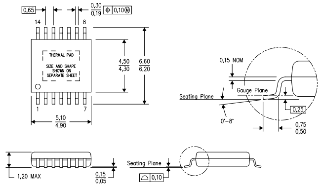
TPS1H100BQPWPRQ1 Manufacturer Information
Texas Instruments emerges as a prominent figure in semiconductor manufacturing, skillfully producing a wide range of components like the TPS1H100BQPWPRQ1 to cater to the insatiable global appetite for electronic devices. Their reputation is strongly tied to their advanced expertise in analog and embedded technologies, which propels an environment rich in continuous innovation. The dynamic nature of their offerings symbolizes a deep commitment to enhancing electronic design and functionality, as they navigate the complexities of the tech landscape. Their product development strategies are intricately linked to global digital transformation initiatives, enabling them to hold a competitive position. Texas Instruments’ prominent status in semiconductor manufacturing is fortified by their persistent emphasis on innovation, the application of state-of-the-art technologies, and a keen alignment with universal industry trends.
Datasheet PDF
TPS1H100BQPWPRQ1 Datasheets:
Symbolization Update 14/Feb/2023.pdf
About us
ALLELCO LIMITED
Read more
Quick inquiry
Please send an inquiry, we will respond immediately.
Frequently Asked Questions [FAQ]
1. What defines the TPS1H100BQPWPRQ1?
The TPS1H100BQPWPRQ1 goes beyond its surface-level technology as a high-side switch equipped with an NMOS power FET and charge pump; it serves as a well-rounded solution tailored for a wide array of applications. Its innovative architecture is geared towards optimizing power management across diverse electronic systems, creating a sense of reliability and efficiency that resonates with contemporary design needs.
2. How many channels are available?
This device is configured as a single-channel entity. Such a streamlined architecture simplifies overall control and seamlessly integrates into space-restricted systems. This characteristic has proven beneficial in environments where minimizing physical footprint and component count drives design success.
3. What are its primary advantages?
The device boasts a range of valuable features including extensive diagnostics and precision current-sense capabilities. These attributes not only elevate performance levels but also empower to monitor system health in time. Such oversight greatly contributes to enhancing the device's durability and reliability.
4. How is reliability ensured?
Reliability is maintained through its programmable current-limit feature. This capability enables to customize the circuit's reactions to faults, embodying a forward-thinking proactive strategy that prepares systems for unforeseen circumstances. Such foresight ultimately contributes to an extended lifespan for the product.
5. What is the high-impedance state of the TPS1H100BQPWPRQ1?
The high-impedance state function supports MCU interface multiplexing. This intentional design allows for multiple pathways in signal processing, which is particularly important in intricate systems that necessitate effective resource management.
6. What is used for version A of the digital status report?
Version A employs an open-drain digital reporting system. This design choice aligns with a popular strategy in modern electronics, where straightforward yet effective signaling methods are preferred. This approach reduces complexity while promoting compatibility across various digital platforms.
7. What happens during fault detection in open-drain?
During fault detection, the system pulls to GND. This mechanism creates a transparent and definitive response to fault conditions, which plays a role in preserving system integrity and preventing cascades of failures.
8. What is essential for matching MCU levels?
To achieve compatibility with MCU levels, a pullup resistor rated at 3.3V or 5V is necessary. This considerate approach to voltage levels highlights a fundamental principle of ensuring component compatibility, an aspect that contributes to optimal system performance while diminishing potential operational conflicts.
9. How is diagnostic precision achieved?
High-accuracy current sensing is key to achieving diagnostic precision. By utilizing advanced sensing technologies, systems can present reliable performance metrics, thus facilitating prompt interventions and maintenance actions that prevent future failures.
10. What gets represented on the CS pin?
The CS pin conveys 1/K of the load current within a voltage range of 0 to 4V. This representation transcends mere numerical data; it acts as an important tool for monitoring, aiding in the evaluation of load conditions and comprehensive system performance.
11. How can the application adjust current limits?
The application allows for current limits to be modified through external high-accuracy current setting. This adaptability grants system the capability to precisely tailor the device’s operational parameters according to specific application needs, mirroring broader trends toward customization in today’s electronics landscape.
12. What feature enhances system reliability?
Managing inrush currents when devices are activated or during fault conditions boosts the system's overall reliability. This capability mitigates stress on components, reflecting a common principle in many successful designs prioritizing satisfaction and component durability amidst varied operational environments.
13. How does the TPS1H100BQPWPRQ1 aid cost reduction?
The TPS1H100BQPWPRQ1 contributes to cost reduction by optimizing component requirements. This engineering approach not only reduces initial costs but also streamlines supply chains, emphasizing the role of efficient resource management in establishing competitive advantages.
14. What is an embedded feature of this switch?
An internally embedded current limiting function enhances the overall functionality of this switch. This built-in feature is gaining popularity in contemporary designs, acknowledging that integrated protections foster confidence and bolster product reliability.
15. What determines the current-limit value?
The setting of the current-limit value relies on whichever setting, internal or external is lower. This dual-option approach offers granular control over operational limits, underlining a design philosophy that champions flexibility and defined parameters tailored to diverse application contexts.
All About TL594: Features, Design, and Uses
on November 20th
What Makes the DL4004 a Reliable Choice
on November 20th
Popular Posts
-
What is GND in the circuit?
on January 1th 3291
-

RJ-45 Connector Guide: RJ-45 Connector Color Codes, Wiring Schemes, R-J45 Applications, RJ-45 Datasheets
on January 1th 2826
-
Understanding Power Supply Voltages in Electronics VCC, VDD, VEE, VSS, and GND
on November 20th 2687
-

Fiber Connector Types: SC Vs LC And LC Vs MTP
on January 1th 2271
-

Comparison Between DB9 and RS232
on January 1th 1891
-

What Is An LR44 Battery?
Electricity, that ubiquitous force, quietly permeates every aspect of our daily lives, from trivial gadgets to life-threatening medical equipment, it plays a silent role. However, truly grasping this energy, especially how to store and efficiently output it, is no easy task. It is against this background that this article will focus on a type of coin cell battery that may seem insignificant on the...on January 1th 1849
-

What Is RF and Why Do We Use It?
Radio Frequency (RF) technology is a key part of modern wireless communication, enabling data transmission over long distances without physical connections. This article delves into the basics of RF, explaining how electromagnetic radiation (EMR) makes RF communication possible. We will explore the principles of EMR, the creation and control of RF signals, and their wide-ranging uses. The article ...on January 1th 1818
-
Understanding the Fundamentals:Inductance Resistance, andCapacitance
In the intricate dance of electrical engineering, a trio of fundamental elements takes center stage: inductance, resistance, and capacitance. Each bears unique traits that dictate the dynamic rhythms of electronic circuits. Here, we embark on a journey to decipher the complexities of these components, to uncover their distinct roles and practical uses within the vast electrical orchestra. Inductan...on January 1th 1817
-

CR2430 Battery Comprehensive Guide: Specifications, Applications and Comparison to CR2032 Batteries
What is CR2430 battery ?Benefits of CR2430 BatteriesNormCR2430 Battery ApplicationsCR2430 EquivalentCR2430 VS CR2032Battery CR2430 SizeWhat to look for when buying the CR2430 and equivalentsData Sheet PDFFrequently Asked Questions Batteries are the heart of small electronic devices. Among the many types available, coin cells play a crucial role, commonly found in calculators, remote controls, and ...on January 1th 1806
-
Comprehensive guide to hFE in transistors
Transistors are crucial components in modern electronic devices, enabling signal amplification and control. This article delves into the knowledge surrounding hFE, including how to select a transistor's hFE value, how to find hFE, and the gain of different types of transistors. Through our exploration of hFE, we gain a deeper understanding of how transistors work and their role in electronic circu...on November 20th 1796


