S9015 PNP Transistor: Equivalent Models, Structural Insights, and C9015 Comparison
This article covers what makes S9015 transistor important in electronics. We’ll start with its background and real-life uses, then look at its technical details, like how it’s built and works. It discuss the features, such as being energy-efficient and quiet, its pin layout and share practical examples, showing how it works in things like audio and signal processing. It will compare to similar transistors and share tips for using it effectively in your circuit designs.Catalog
S9015 Transistor Overview
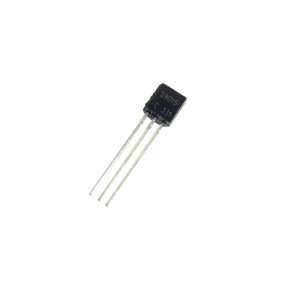
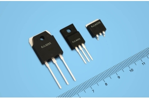
The S9015, a low-power NPN transistor in a TO-92 package, stands out for its capacity to handle a 100mA collector current and a 50V collector-emitter voltage. This transistor, often used alongside the S9014, boasts high gain, low noise, and an exceptional high-frequency response. These features make it adept for switching, amplification, and voltage stabilization within various circuits.
Replacements and Equivalents
• BC557C
• S8550
• S9014
• SS9012
• MPSW55
• 2N4403
Design and Operational Mechanics of the S9015 Transistor
Physical Structure
The S9015 transistor comprises a PNP-type emitter junction along with an NPN-type collector junction. The emitter junction's N region directly connects to the base, while the collector junction’s N region interfaces with the emitter.
Functionality of Junctions
This configuration facilitates the control of current flow and the amplification of signals through the S9015 transistor.
Base Current and Saturation
When the base current exceeds the saturation current flowing between the emitter and collector, the transistor transitions into an amplified state. This state is governed by the current gain, elaborates on the interaction between the emitter and collector currents.
Current Gain and Applications
The current gain can be finely adjusted to optimize the transistor's performance in various applications, including audio amplification, and signal processing.
Electron Movement Mechanisms
Electron diffusion within its PN junctions refers to the migration of charge carriers from high to low concentration regions, while electron drift involves the movement of electrons under the influence of an electric field. These electro-physical phenomena ensure the transistor reliably functions for circuit amplification and switching roles.
S9015 Transistor Pinout Configuration
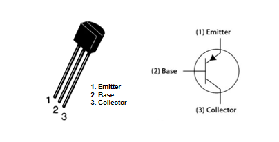
Emitter
The emitter influences the functionality of the S9015 transistor. Connecting it to the circuit's negative terminal, it serves as the source of charge carriers. It facilitates the release of electrons (for NPN transistors) or holes (for PNP transistors), maintaining current flow through the transistor.
Base
The base controls the operation of the S9015 transistor, linked to the control signal source. It regulates the current flow between the emitter and collector. A small current at the base can control a larger current flow from collector to emitter, amplifying the signal.
Collector
The collector connects to the circuit's positive terminal, managing the output current. Its connection to the load allows the transistor to function as a switch or amplifier, depending on the application.
S9015 Transistor Features
Energy Efficiency
The S9015 transistor stands out for its efficient low-power design. This feature minimizes energy consumption, extending battery life in portable devices for modern, on-the-go lifestyles.
Noise Reduction in Audio
Another aspect is its capacity to reduce noise levels. This ability becomes advantageous in audio amplification, ensuring clearer and more accurate sound reproduction.
Signal Processing
The S9015's versatility makes it an asset in various electronic applications. It finds utility in signal processing, where clear and precise signals are required.
Switching Operations
In switching operations, its powerful electrical characteristics ensure reliable performance across different circuit configurations. This reliability simplifies the design process for engineers by providing a stable and predictable component.
Amplification Circuits
Its flexibility also extends to amplification circuits, where its consistent performance is prized. You can count on the S9015 to handle diverse requirements with ease.
High Current Gain
The high current gain of the S9015 is beneficial for circuits that demand considerable amplification. This parameter is use in applications where small input signals need to be amplified to larger output signals, such as in radio frequency and audio equipment.
Specifications of the S9015 Transistor
Input Resistance
The input resistance of the S9015 transistor ranges from 1.2kΩ to 10kΩ. This variance suggests that the transistor requires minimal current inputs. Such efficiency benefits applications focusing on conserving input signal power. Low-power signal amplification in various circuits is notably improved by this property, making it highly desirable in delicate and sensitive electronic designs.
Output Resistance
The output resistance of the S9015 transistor lies between 1kΩ and 10kΩ. This range determines the output current capability and influences how well the transistor can handle specified loads without substantial power loss. Keeping this parameter in mind during design can enhance overall device performance and ensure maintained signal integrity for electronics needing stable output dynamics.
Maximum Frequency
Operating up to frequencies of 150MHz, the S9015 transistor is well-suited for RF amplifiers and oscillators, which are important components in communication devices. Implementing this transistor in RF designs showcases its potential to maintain stable performance at high operational frequencies. Such stability ensures dependable and clear communication signals, forming the backbone of efficient communication systems.
Maximum Current
The S9015 transistor accommodates a maximum collector current of 100mA. Surpassing this current can lead to device failure or reduce the lifespan. Adhering to this current limit ensures reliable functionality and prolonged durability, allowing electronic devices to perform consistently without premature breakdowns.
Maximum Power Consumption
The S9015 transistor can consume up to 400mW of power. Integrating effective thermal management techniques, like using heat sinks, is great to prevent overheating. Efficient thermal dissipation in real-world applications preserves device performance and avoids failures caused by excessive heat. Neglecting proper heat management could jeopardize the functionality and efficiency of the transistor.
Maximum Voltage
The transistor supports a collector-emitter voltage up to 45V. This parameter delineates its operational ceiling, beyond which the transistor risks breakdown. You must ensure voltage levels stay within this limit to avoid damage. Implementing strong voltage regulation strategies extends the operational lifespan of the transistor by shielding it from voltage-induced harm.
Amplification
The DC amplification factor of the S9015 transistor ranges from 70 to 400. This broad spectrum provides substantial current output gain, suitable for diverse amplification needs. In applications such as audio amplification, this characteristic is harnessed to effectively boost signal strength. This amplification capability highlights the versatility and function of the S9015 in multiple electronic solutions.
Maximum Ratings and Electrical Specifications of the S9015 Transistor
Maximum Ratings
Delving into the maximum ratings of the S9015 transistor requires more than just understanding them; it’s about nurturing the habits of safely operating within these limits. These ratings delineate the boundaries where the transistor can function without harm. Through the lens of practical experience, maintaining operations within these confines is best for achieving a strong and reliable design. Exceeding these ratings can precipitate thermal issues, erode performance, and eventually spell the end for the component.
|
Parameter |
Symbol |
Rating |
Unit |
|
Collector-Base Voltage |
VCBO |
-50 |
V |
|
Collector-Emitter Voltage |
VCEO |
-45 |
V |
|
Emitter-Base Voltage |
VEBO |
-5 |
V |
|
Collector Current–Continuous |
IC |
-0.1 |
A |
|
Collector Power Dissipation |
PC |
0.2 |
W |
|
Junction Temperature |
Tj |
150 |
°C |
|
Storage Temperature |
Tstg |
-55 to 150 |
°C |
Electrical Characteristics
Examining the electrical characteristics of the S9015 transistor imparts a deeper comprehension of its behavior under fixed conditions. Among these characteristics are several important parameters like current gain, saturation voltages, and leakage currents. These parameters are invaluable for circuit design and fine-tuning.
|
Parameter |
Symbol |
Test Conditions |
Min |
Typ |
Max |
Unit |
|
Collector-base breakdown voltage |
VCBO |
IC=-100μA, IE=0 |
-50 |
V |
||
|
Collector-emitter breakdown voltage |
VCEO |
IC=-1mA, IB=0 |
-45 |
V |
||
|
Emitter-base breakdown voltage |
VEBO |
IE=-100 μA, IC=0 |
-5 |
V |
||
|
Collector cutoff current |
ICBO |
VCB=-50V, IE=0 |
|
-0.1 |
μA |
|
|
Emitter cutoff current |
IEBO |
VEB=-5V, IC=0 |
|
-0.1 |
μA |
|
|
DC current gain |
hFE |
VCE=-5V, IC=-1mA |
200 |
1000 |
||
|
Collector-emitter saturation voltage |
VCE(sat) |
IC=-100mA, IB=-10mA |
|
-0.3 |
V |
|
|
Base-emitter saturation voltage |
VBE(sat) |
IC=-100mA, IB=-10mA |
|
-1 |
V |
|
|
Transition frequency |
fT |
VCE=-5V, IC=-10mA, f=30MHz |
150 |
MHz |
Comparing the S9015 and C9015 Transistors
The S9015 and C9015 transistors, both categorized as low-power transistors, have unique characteristics that merit detailed attention.
Electrical Parameters
The maximum rated current and voltage of S9015 and C9015 exhibit slight variations. The S9015 boasts a maximum collector current of 500mA and a collector-emitter voltage of 45V. The C9015, depending on its production details, might differ in these ratings.
Polarity Differences
A distinction is their polarity. The S9015 is an NPN transistor, while the C9015 is a PNP transistor. NPN transistors like the S9015 usually source current from the collector to the emitter, fittingly used in low-side switching applications. PNP transistors such as the C9015 source current from the emitter to the collector, ideal for high-side switching. This distinction means that you need to thoroughly understand these roles to prevent misconfigurations, that could result in circuit failures or less-than-optimal performance.
Packaging and Handling
The S9015 comes in the TO-92 package, which offers ease of handling and effective heat dissipation, suitable for traditional through-hole assembly. The C9015, however, is commonly found in the SOT-23 package, more compact and adapted for contemporary surface-mount technology. This difference in packaging can influence decisions regarding PCB layout and thermal management strategies.
Applications
The applications for S9015 and C9015 diverge noticeably. The S9015 excels in switching power supplies and motor drives, owing to its NPN nature and strong current-handling capacity, making it ideal for dynamic loads and power conversion stages. On the other hand, the C9015, being a PNP transistor, is suited for LED drives and power conversion. Its high-side switching capability ensures steady and efficient power delivery to sensitive components like LEDs.
Differences Among the S9015, S9013, and S9014 Transistors
Maximum Collector Current
The distinctions among the transistors, S9013, S9014, and S9015, for selecting the appropriate component in electronic designs differ in maximum collector current, current amplification factors, voltage ratings, and their applications. For those needing higher current throughput, the S9013 proves advantageous, handling up to 500 mA. This capacity makes it ideal for applications with higher current demands. In contrast, the S9014 and S9015 support a maximum of 100 mA, making them better suited for lower current applications. This variance often guides the choice of transistor based on the circuit's current requirements.
Current Amplification Factors (hFE)
Current amplification factor, denoted as hFE, defines a transistor's ability to amplify current. The S9013 offers an hFE range of 40 to 400, providing a broad spectrum of amplification potential. The S9014 presents a more moderate range of 60 to 300. The S9015, with its hFE range of 120 to 450, exhibits the highest amplification potential, making it preferable for applications requiring signal enhancement.
Voltage Ratings
Voltage rating distinctions are also notable. The VCEO (collector-emitter voltage) for the S9013 stands at 40V. The S9014 can tolerate up to 45V. The S9015 can handle up to 50V. The S9015 is more strong in terms of voltage, suiting applications with higher voltage demands better.
Applications
The S9013 is an NPN transistor, optimal for low-power applications, leveraging its higher current rating for such tasks. Both the S9014 and S9015 are PNP transistors, suited for similar low-power scenarios. However, the S9015 shines in medium and low power amplification tasks due to its higher voltage and current amplification capabilities. Therefore, the choice between these transistors often hinges on the project's specific needs, particularly in terms of amplification factor and voltage tolerance.
Applications of the S9015 Transistor
The S9015 transistor exhibits a captivating blend of adaptability and reliability, rendering it appropriate for a multitude of applications. These encompass voltage regulation, inverting circuits, power management, RF amplification, signal amplification, signal conditioning, and sensor interfaces. Each application area is elaborated below, detailing its functionality.
Voltage Regulation
Embedded in voltage regulation circuits, the S9015 transistor ensures a stable output voltage. It capably maintains output consistency despite input voltage or load condition fluctuations. This functionality bolsters the operational dependability of electronic devices and contributes to their enhanced longevity and performance by providing steadfast voltage regulation.
Inverting Circuits
In inverting circuits, the S9015 transistor is good for altering the phase of an input signal. This role is use for various signal processing tasks needing phase reversal. This results in more accurate and trustworthy signal transmission.
Power Management
The S9015 transistor excels in controlling and distributing power with finesse. It finds applications in power management ICs and modules, optimizing power usage and extending battery life in portable devices. Efficient power management via the S9015 translates into meaningful enhancements in device efficiency and heat dissipation, fostering a more balanced performance.
RF Amplification
Within the realm of RF amplification, the S9015 transistor excels in boosting radio frequency signal strength. Its design masterfully curtails the noise figure, an important factor in applications where clear and signal transmission. Utilizing the S9015 in RF amplification fortifies systems, achieving superior range and communication clarity.
Signal Amplification
High gain and low noise performance make the S9015 a stellar candidate for signal amplification tasks. It is frequently employed in audio equipment, communication devices, and other electronic circuits where weak signal enhancement is required. The outcome of deploying the S9015 in signal amplification is manifested in clearer audio experiences and more reliable data transmission.
Signal Conditioning
In signal conditioning, the role of the S9015 transistor involves refining signals to render them suitable for additional processing. It plays an active part in filtering, amplifying, and converting signals to desired levels, which enhances overall system accuracy. Practical implementations reveal that incorporating the S9015 in signal conditioning circuits results in more precise data acquisition and improved system responsiveness.
Sensor Interfaces
The S9015 transistor is instrumental in sensor interfaces, facilitating the connection between sensors and microcontrollers or different processing units. It assists in amplifying and conditioning sensor outputs, ensuring precise readings and optimal signal levels. The real-world usage of the S9015 in sensor interfaces frequently leads to heightened measurement accuracy and fortified system stability.
Frequently Asked Questions [FAQ]
1. What is the S9015 transistor used for?
The S9015 transistor exhibits remarkable versatility, fitting seamlessly into a multitude of applications:
Audio Preamplification: Enhancing weak audio signals before they reach the main amplifier.
Signal Amplification: Amplifying signals with variable gains to achieve desired levels.
Switching Tasks: Effectively controlling relays and LEDs by toggling currents.
Analog and Digital Circuits: Operating efficiently within both analog and digital environments.
2. What is the main purpose of a transistor?
A transistor primarily amplifies current within a circuit. Current amplification, transforms a small input current into a substantially larger output current. Signal processing and power regulation, eEnhances a wide range of applications by improving the signals and maintaining power consistency. With time, advancements have positioned transistors as good in nearly every electronic device, boosting overall performance and efficiency.
3. What is the common applications of the S9015 transistor?
Signal Amplification: Central to tasks like boosting weak audio signals in amplifiers.
Switching: Controls electrical flows within circuits.
Voltage Regulation: Helps keep output voltage stable in voltage regulators.
4. How to check if the S9015 transistor is good?
To assess an S9015 transistor's condition, use a multimeter set to measure resistance. Connect the multimeter leads to the transistor's terminals. Observe the readings. Readings should not approach infinity or be excessively low. Extremes suggest potential damage or malfunction.
5. Can the S9015 transistor be used as a switch?
The S9015 transistor effectively functions as a switch by toggling between cutoff (off) and saturation (on) modes. Current control manages current flow between the collector and emitter. Circuit operations enables or disables electrical flow as needed. This switching capability is extensively utilized in electronic systems, facilitating a range of control mechanisms across various circuit operations.
About us
ALLELCO LIMITED
Read more
Quick inquiry
Please send an inquiry, we will respond immediately.
Guide to the LM339AN Quad Voltage Comparator
on September 27th
TL3845P PWM Controller: Pinout, Key Features, and Layout Tips
on September 27th
Popular Posts
-
What is GND in the circuit?
on January 1th 3140
-

RJ-45 Connector Guide: RJ-45 Connector Color Codes, Wiring Schemes, R-J45 Applications, RJ-45 Datasheets
on January 1th 2687
-
Understanding Power Supply Voltages in Electronics VCC, VDD, VEE, VSS, and GND
on November 15th 2256
-

Fiber Connector Types: SC Vs LC And LC Vs MTP
on January 1th 2194
-

Comparison Between DB9 and RS232
on January 1th 1806
-

What Is An LR44 Battery?
Electricity, that ubiquitous force, quietly permeates every aspect of our daily lives, from trivial gadgets to life-threatening medical equipment, it plays a silent role. However, truly grasping this energy, especially how to store and efficiently output it, is no easy task. It is against this background that this article will focus on a type of coin cell battery that may seem insignificant on the...on January 1th 1781
-
Understanding the Fundamentals:Inductance Resistance, andCapacitance
In the intricate dance of electrical engineering, a trio of fundamental elements takes center stage: inductance, resistance, and capacitance. Each bears unique traits that dictate the dynamic rhythms of electronic circuits. Here, we embark on a journey to decipher the complexities of these components, to uncover their distinct roles and practical uses within the vast electrical orchestra. Inductan...on January 1th 1734
-
What Is RF and Why Do We Use It?
Radio Frequency (RF) technology is a key part of modern wireless communication, enabling data transmission over long distances without physical connections. This article delves into the basics of RF, explaining how electromagnetic radiation (EMR) makes RF communication possible. We will explore the principles of EMR, the creation and control of RF signals, and their wide-ranging uses. The article ...on January 1th 1688
-

CR2430 Battery Comprehensive Guide: Specifications, Applications and Comparison to CR2032 Batteries
What is CR2430 battery ?Benefits of CR2430 BatteriesNormCR2430 Battery ApplicationsCR2430 EquivalentCR2430 VS CR2032Battery CR2430 SizeWhat to look for when buying the CR2430 and equivalentsData Sheet PDFFrequently Asked Questions Batteries are the heart of small electronic devices. Among the many types available, coin cells play a crucial role, commonly found in calculators, remote controls, and ...on January 1th 1687
-
Comprehensive guide to hFE in transistors
Transistors are crucial components in modern electronic devices, enabling signal amplification and control. This article delves into the knowledge surrounding hFE, including how to select a transistor's hFE value, how to find hFE, and the gain of different types of transistors. Through our exploration of hFE, we gain a deeper understanding of how transistors work and their role in electronic circu...on November 15th 1649
HOT Part Number
-

RC1206JR-073R9L
YAGEO
RES 3.9 OHM 5% 1/4W 1206
ADS931E
Texas Instruments
IC ADC 8BIT PIPELINED 28SSOP
350759-5
TE Connectivity AMP Connectors
CONN HDR 2POS 0.25 GOLD PCB
STM32L073V8T6
STMicroelectronics
IC MCU 32BIT 64KB FLASH 100LQFP
SFR9214TM
Fairchild Semiconductor
P-CHANNEL POWER MOSFET
GRM1885C2A7R3CA01D
Murata Electronics
CAP CER 7.3PF 100V C0G/NP0 0603
PIC18F6622-I/PT
Microchip Technology
IC MCU 8BIT 64KB FLASH 64TQFP
ISL6605IRZ
Renesas Electronics America Inc
IC GATE DRVR HALF-BRIDGE 8QFN
MC908QB4CDWE
NXP USA Inc.
IC MCU 8BIT 4KB FLASH 16SOIC
BD8139AEFV-E2
Rohm Semiconductor
IC VID TFT-LCD VOLT REG 40HTSSOP
1B31AN
ADI (Analog Devices, Inc.)
IC SIGNAL COND STRAIN GAUGE 28DI
R2120
Microchip Technology
RECTIFIER
245861040004829+
KYOCERA AVX
RECPT - 0.35MM PITCH - 40 POS 0.
MAX2321EUP
Analog Devices Inc./Maxim Integrated
ADJ, SIGE DUAL-BAND LNA/MIXER
MC100H601FNR2
onsemi
IC TRANSLATOR UNIDIR 28PLCC
MIC5305-1.5YD5
Micrel Inc.
IC REG LINEAR 150MA MICROCAP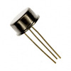
LM117H
Texas Instruments
IC REG LINEAR POS ADJ 1.5A TO3
AD7672KN10
Analog Devices Inc.
IC ADC 12BIT LC2MOS 24-DIP -

RT0603BRE07270RL
YAGEO
RES SMD 270 OHM 0.1% 1/10W 0603
XCKU060-1FFVA1156I
AMD
IC FPGA 520 I/O 1156FCBGA
MAX1982EUT+T
Analog Devices Inc./Maxim Integrated
IC REG LINEAR 1.2V 300MA SOT23-6
PEF20550HV2.1
Infineon Technologies
ELIC LINE CARD INTERFACE
SN75207BN
Texas Instruments
IC RECEIVER 0/2 14DIP
WRF2405S-3WR2
Mornsun America, LLC
ISOLATED MODULE DC DC CONVERTER
EL1883IS
Renesas Electronics America Inc
IC VIDEO SYNC SEPARATOR 8SOIC
NB7VPQ16MMNG
onsemi
IC CML PRE-EMPH DRIVER 16QFN
GRM31B5C2H102JW01L
Murata Electronics
CAP CER 1000PF 500V C0G/NP0 1206
N7G24-A0B2RB-10-3HT
3M
CONN CFAST CARD PUSH-PUSH R/A
PIC16C73A-20I/SO
Microchip Technology
IC MCU 8BIT 7KB OTP 28SOIC
LMV358IDGKR
Texas Instruments
IC OPAMP GP 2 CIRCUIT 8VSSOP
DS2437S
Analog Devices Inc./Maxim Integrated
IC BATT MONITOR SMART 16SSOP
EL4583CSZ
Renesas Electronics America Inc
IC VIDEO SYNC SEPARATOR 16SOIC
1206ZC104MAT2A
KYOCERA AVX
CAP CER 0.1UF 10V X7R 1206
VI-B63-MU-BM
Vicor Corporation
VI-B63-MU-BM 300V / 24V 200W
MC56F82733VFM
NXP USA Inc.
IC MCU 32BIT 48KB FLASH 32QFN
26PCAFA6D
Honeywell Sensing and Productivity Solutions
SENSOR 1PSID 0.2" .0167V -
LTC3255IMSE#PBF
Analog Devices Inc.
IC REG CHARGE PUMP ADJ 10MSOP
SMLZ14BGTT86
Rohm Semiconductor
LED BLUE CLEAR P-LCC-2 SMD
UCC39151DP
Texas Instruments
IC SUPERVISOR PWR SUP SUPPORT
PEB3332HTV2.1
Lantiq
VINETIC VOICE AND INTERNET ENHAN
CL10B272KB8SFNC
Samsung Electro-Mechanics
CAP CER 2700PF 50V X7R 0603
MLG0603P3N6ST000
TDK Corporation
FIXED IND 3.6NH 400MA 200MOHM SM
MLZ2012N2R2LT000
TDK Corporation
FIXED IND 2.2UH 800MA 120MOHM SM
STCC2539IQTR
STMicroelectronics
IC PWR SWITCH N-CH 1:1 16VFQFPN
XC6222D481ER-G
Torex Semiconductor Ltd
IC REG LINEAR 4.8V 700MA 6USPC
DM74ALS138MX
onsemi
IC DECODER/DEMUX 1X3:8 16SOIC
08055C472KAT2P
KYOCERA AVX
CAP CER 4700PF 50V X7R 0805
SMBJ170CA
Yangjie Technology
SMB 600W 275V 2.18A TVS Diodes
ADP196ACBZ-R7
Analog Devices Inc.
IC PWR SWITCH N-CHAN 1:1 6WLCSP
LAA110S
IXYS Integrated Circuits Division
SSR RELAY SPST-NO 120MA 0-350V
LM5141RGER
Texas Instruments
LM5141RGER
LTC4151CMS#PBF
Analog Devices Inc.
IC CURRENT MONITOR(12BIT) 10MSOP
NJM2882F25-TE1
Nisshinbo Micro Devices Inc.
IC REG LINEAR 2.5V 300MA SOT23-5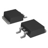
15TQ060STRR
Vishay General Semiconductor - Diodes Division
DIODE SCHOTTKY 60V 15A TO263AB