Complete Guide to the ARM7-Based LPC2148 Microcontroller
Embedded system design requires selecting the right microprocessor cores and development tools to specific project needs. The ARM processor is a great choice in this field due to its versatility across various industries, from mobile technology to automotive systems. This article focuses on the ARM7-based LPC2148 microcontroller, known for its strong and adaptability. We will delve into its architecture and pin configuration, providing insights into its functionalities and potential applications.Catalog
What is the ARM7-Based (LPC2148) Microcontroller?
ARM represents a prominent 32-bit RISC architecture developed by ARM Holdings, serving as a core platform in microprocessor design. Its efficiency and adaptability have made it appealing across a wide range of applications. The widespread licensing of this architecture has enabled numerous companies to create innovative ARM-based products catering to diverse markets, driven by both ambition and necessity.
Key semiconductor players such as Samsung and TI actively create systems-on-chip (SOCs) that utilize ARM architecture, their dedication to this tech. This trend reveals ARM's capability to meet the evolving needs of sophisticated consumer electronics, industrial machinery, and more. Observations in market dynamics show ARM's flexible traits are a great influence in its integration into the latest tech products.
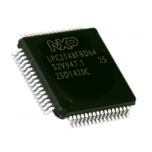
The ARM7-based LPC2148 microcontroller is celebrated for its efficiency and low power footprint. It finds extensive use in everyday applications like automotive systems and portable electronics. ARM architecture uniquely balances simplicity with computational power. The instruction set is crafted to be intuitive, allowing for efficient execution and reduced development time. This ideology suggests that simplicity enhances rather than detracts from capability, streamlining product development by making debugging and maintenance more straightforward.
The ARM7 Processor
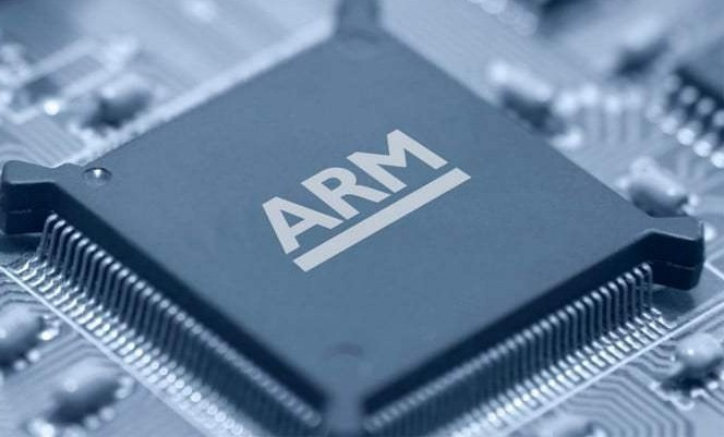
Embedded systems find the ARM7 processor an appealing choice due to how it harmonizes classical processing methods with the evolving Cortex architectures. Its appeal stems from its adeptness at handling diverse tasks, serving both older technologies and pioneering advancements with equal finesse. The ARM7 processor is complemented by extensive documentation provided by companies like NXP Semiconductors. This plethora of resources aids newcomers as they nurture their skills in hardware and software design. The lucid guidance facilitates an easier learning curve.
ARM7 processors are frequently utilized in consumer electronics, automotive controls, and industrial systems. Their capacity to manage an array of tasks from straightforward calculations to intricate system administration earns them appreciation in fields where dependability and economic efficiency are valued. Interacting with ARM7 microcontrollers allows individuals to enhance both theoretical knowledge and hands-on skills. Crafting systems using these processors cultivates an appreciation for streamlined coding and adept resource management, often sparking creative approaches to problem-solving. The ARM7 architecture offers a connection between conventional processing techniques and modern-day demands, maintaining its importance in current technology.
The LPC2148 Microcontroller
The LPC2148 microcontroller, crafted by NXP, embodies a suite of features in search of versatile and reliable solutions. Operating on a 16-bit or 32-bit ARM7 processor core, it caters to a spectrum of applications, revealing both adaptability and resilience.
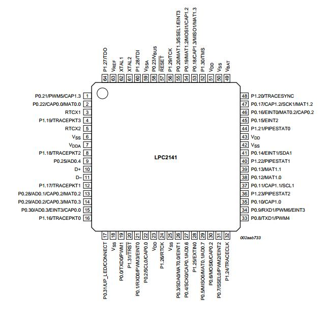
Packaging and Programming
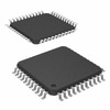
Encased in a sleek LQFP64 package, the LPC2148 integrates effortlessly into diverse designs. It supports both in-system and in-application programming, providing the allure of updating firmware without extraction from the circuit board. This eases the burden for remote devices needing frequent updates to sustain peak performance and safeguard security.
Memory and Speed
Offering up to 40KB of SRAM and 512KB of flash memory, the LPC2148 opens possibilities for managing intricate programs and data. Operating at speeds up to 60 MHz, it meets the demands of applications that thrive on rapid data processing and real-time responsiveness.
Connectivity and Interfaces
With a full-speed USB 2.0 controller, the LPC2148 ensures swift data transfer and seamless connectivity with other digital systems. This feature emerges as a linchpin for communication.
Analog and Digital Conversions
Incorporating ADCs, DAC, and multiple timers, it excels in precise analog and digital signal processing, rendering it ideal for embedded systems focused on accurate sensor readings and control tasks. The low-power RTC and various serial interfaces guarantee consistent timekeeping and adaptable communication capabilities.
Power Management and Efficiency
Tailored for energy-sensitive applications, the LPC2148 champions power-saving modes, features 5V-tolerant I/O, and offers multiple interrupt options. Its Phase Locked Loop for clock control harmonizes power efficiency while curbing system noise for devices relying on batteries.
LPC2148 Microcontroller Memory Architecture
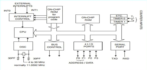
The LPC2148 microcontroller presents a diverse memory setup with 512KB of flash memory and 32KB of SRAM. Ideal for various embedded applications, it supports multiple programming approaches, fostering stable data retention over time.
On-chip Flash Memory
On-chip flash memory interfaces with JTAG and UART, among others, providing adaptability in programming and debugging. The robust endurance of this memory supports frequent write-erase cycles, which is valuable for scenarios demanding regular firmware updates or data logging. Its consistent performance nurtures reliability across these tasks.
On-chip SRAM
With 32KB of SRAM, this component manages different data widths, making it suitable for intricate data operations and effective multitasking. Temporary data storage during high-speed processing is smoothly handled by the SRAM, enhancing system efficiency and responsiveness.
Input/Output Ports
The LPC2148 has two adaptable I/O ports, configurable for functions such as GPIO and UART. This flexibility addresses shifting application requirements, aiding seamless project integration as needs evolve. This feature optimize communication protocols and boost system adaptability.
Initiating Effective Programming Strategies
GPIO pins fulfill multiple roles in various applications. Ports P0 and P1, known for their adaptability, include pins that remain inaccessible their management hinges on specific register groups, offering a canvas for personalized configurations. Ports P0 and P1 unfold extensive functionality, catering to diverse electronics and computing projects. Their adaptability invites users to delve into the hardware's potential, demanding an appreciation of its intricate workings. Engaging hands-on with these configurations enriches one's capability to navigate and resolve complex scenarios. Register groups manage the customization of otherwise unreachable pins, aligning with unique application demands. They allow for dynamic alterations, a notion for performance refinement. Skillful handling of these configurations achieves a harmonious balance between operational needs and resource management.
ARM7-Based (LPC2148) Pin Configuration
|
Pin Number |
Pin Name/Function |
Description |
|
1 |
P0.21 / PWM5 / CAP1.3 / AD1.6 |
GPIO, PWM output 5, Timer 1 Capture 3, ADC input 6
(LPC2144/46/48) |
|
2 |
P0.22 / CAP0.0 / AD1.7 / MAT0.0 |
GPIO, Timer 0 Capture 0, ADC input 7 (LPC2144/46/48),
Timer 0 Match 0 |
|
3 |
RTXC1 |
Input to RTC oscillator circuit |
|
4 |
TRACEPKT3 / P1.19 |
Trace packet 3, GPIO |
|
5 |
RTXC2 |
Output from RTC oscillator circuit |
|
6, 18, 25, 42, 50 |
Ground (GND) |
Ground reference pins |
|
7 |
VDDA |
Analog voltage power supply (3.3V) |
|
8 |
P1.18 / TRACEPKT2 |
GPIO, Trace packet 2 |
|
9 |
P0.25 / AOUT / AD0.4 |
GPIO, DAC output (LPC2142, 2144, 2146, 2148), ADC input 4 |
|
10 |
D+ |
USB D+ line |
|
11 |
D- |
USB D- line |
|
12 |
P1.17 / TRACEPKT1 |
GPIO, Trace packet 1 |
|
13 |
P0.28 / CAP0.2 / AD0.1 / MAT0.2 |
GPIO, Timer 0 Capture 2, ADC input 1, Timer 0 Match 2 |
|
14 |
P0.29 / CAP0.3 / AD0.2 / MAT0.3 |
GPIO, Timer 0 Capture 3, ADC input 2, Timer 0 Match 3 |
|
15 |
P0.30 / EINT3 / AD0.3 / CAP0.0 |
GPIO, External Interrupt 3, ADC input 3, Timer 0 Capture
0 |
|
16 |
P1.16 / TRACEPKT0 |
GPIO, Trace packet 0 |
|
17 |
P0.31 / UP_LED / CONNECT |
GPIO, USB uplink status LED, Soft Connect feature control |
|
19 |
P0.0 / PWM1 / TXD0 |
GPIO, PWM output 1, UART0 TX |
|
20 |
P1.31 / TRST |
GPIO, JTAG test reset |
|
21 |
P0.1 / PWM3 / RXD0 / EINT0 |
GPIO, PWM output 3, UART0 RX, External Interrupt 0 |
|
22 |
P0.2 / CAP0.0 / SCL0 |
GPIO, Timer 0 Capture 0, I2C0 clock |
|
23, 43, 51 |
VDD |
Power supply voltage for I/O ports and the core |
|
24 |
P1.26 / RTCK |
GPIO, Return test clock for JTAG |
|
26 |
P0.3 / SDA0 / MAT0.0 / EINT1 |
GPIO, I2C0 data, Timer 0 Match 0, External Interrupt 1 |
|
27 |
P0.4 / CAP0.1 / SCK0 / AD0.6 |
GPIO, Timer 0 Capture 1, SPI clock, ADC input 6 |
|
28 |
P1.25 / EXTIN0 |
GPIO, External trigger input |
|
29 |
P0.5 / MAT0.1 / MISO0 / AD0.7 |
GPIO, Timer 0 Match 1, SPI MISO, ADC input 7 |
|
30 |
P0.6 / MOSI0 / CAP0.2 / AD1.0 |
GPIO, SPI MOSI, Timer 0 Capture 2, ADC input 0
(LPC2144/46/48) |
|
31 |
P0.7 / PWM2 / SSEL0 / EINT2 |
GPIO, PWM output 2, SPI slave select, External Interrupt
2 |
|
32 |
P1.24 / TRACECLK |
GPIO, Trace clock |
|
33 |
P0.8 / TXD1 / PWM4 / AD1.1 |
GPIO, UART1 TX, PWM output 4, ADC input 1 (LPC2144/46/48) |
|
34 |
P0.9 / PWM6 / RXD1 / EINT3 |
GPIO, PWM output 6, UART1 RX, External Interrupt 3 |
|
35 |
P0.10 / RTS1 / CAP1.0 / AD1.2 |
GPIO, UART1 RTS, Timer 1 Capture 0, ADC input 2
(LPC2144/46/48) |
|
36 |
P1.23 / PIPESTAT2 |
GPIO, Pipeline status bit 2 |
|
37 |
P0.11 / CAP1.1 / CTS1 / SCL1 |
GPIO, Timer 1 Capture 1, UART1 CTS, I2C1 clock |
|
38 |
P0.12 / MAT1.0 / AD1.3 / DSR1 |
GPIO, Timer 1 Match 0, ADC input 3 (LPC2144/46/48), UART1
DSR |
|
39 |
P0.13 / DTR1 / MAT1.1 / AD1.4 |
GPIO, UART1 DTR, Timer 1 Match 1, ADC input 4
(LPC2144/46/48) |
|
40 |
P1.22 / PIPESTAT1 |
GPIO, Pipeline status bit 1 |
|
41 |
P0.14 / DCD1 / EINT1 / SDA1 |
GPIO, UART1 DCD, External Interrupt 1, I2C1 data |
|
44 |
P1.21 / PIPESTAT0 |
GPIO, Pipeline status bit 0 |
|
45 |
P0.15 / EINT2 / RI1 / AD1.5 |
GPIO, External Interrupt 2, UART1 RI, ADC input 5
(LPC2144/46/48) |
|
46 |
P0.16 / MAT0.2 / EINT0 / CAP0.2 |
GPIO, Timer 0 Match 2, External Interrupt 0, Timer 0
Capture 2 |
|
47 |
P0.17 / SCK1 / CAP1.2 / MAT1.2 |
GPIO, SSP SCK, Timer 1 Capture 2, Timer 1 Match 2 |
|
48 |
P1.20 / TRACESYNC |
GPIO, Trace synchronization signal |
|
49 |
VBAT |
Power supply for the RTC |
|
52 |
P1.30 / TMS |
GPIO, Test mode select for JTAG |
|
53 |
P0.18 / CAP1.3 / MISO1 / MAT1.3 |
GPIO, Timer 1 Capture 3, SSP MISO, Timer 1 Match 3 |
|
54 |
P0.19 / MOSI1 / MAT1.2 / CAP1.2 |
GPIO, SSP MOSI, Timer 1 Match 2, Timer 1 Capture 2 |
|
55 |
P0.20 / SSEL1 / MAT1.3 / EINT3 |
GPIO, SSP Slave Select, Timer 1 Match 3, External
Interrupt 3 |
|
56 |
P1.29 / TCK |
GPIO, Test clock for JTAG |
|
57 |
External Reset Input |
Resets the device to default conditions |
|
58 |
P0.23 / VBUS |
Indicates the presence of USB bus power |
|
59 |
VSSA |
Analog ground, separated to reduce noise and error |
|
60 |
P1.28 / TDI |
GPIO, Test data input for JTAG |
|
61 |
XTAL2 |
Output from the oscillator amplifier |
|
62 |
XTAL1 |
Input to the internal clock generator and oscillator
circuits |
|
63 |
VREF-ADC Reference |
Nominal voltage for ADC reference, separated to reduce
error and noise |
|
64 |
P1.27 / TDO |
GPIO, Test data output for JTAG |
Conclusion
The ARM7-based LPC2148 microcontroller serves as a dynamic and adaptable platform for developing embedded systems. The LPC2148 is favored in diverse fields such as consumer electronics and industrial automation due to its flexible architecture. This flexibility invites exploration and innovation. Its capabilities extend from handling simple tasks to executing complex operations, showcasing its versatile nature. The LPC2148 remains a preferred tool for its lasting impact in an ever-changing tech sector.
About us
ALLELCO LIMITED
Read more
Quick inquiry
Please send an inquiry, we will respond immediately.
STM32L vs STM32F: A Comprehensive Guide to Their Differences and Applications
on October 2th

13009D Transistor Explained: Specs, Applications, and Equivalent Models
on October 1th
Popular Posts
-

What is GND in the circuit?
on January 1th 2933
-

RJ-45 Connector Guide: RJ-45 Connector Color Codes, Wiring Schemes, R-J45 Applications, RJ-45 Datasheets
on January 1th 2488
-

Fiber Connector Types: SC Vs LC And LC Vs MTP
on January 1th 2080
-
Understanding Power Supply Voltages in Electronics VCC, VDD, VEE, VSS, and GND
on November 8th 1874
-

Comparison Between DB9 and RS232
on January 1th 1759
-

What Is An LR44 Battery?
Electricity, that ubiquitous force, quietly permeates every aspect of our daily lives, from trivial gadgets to life-threatening medical equipment, it plays a silent role. However, truly grasping this energy, especially how to store and efficiently output it, is no easy task. It is against this background that this article will focus on a type of coin cell battery that may seem insignificant on the...on January 1th 1709
-
Understanding the Fundamentals:Inductance Resistance, andCapacitance
In the intricate dance of electrical engineering, a trio of fundamental elements takes center stage: inductance, resistance, and capacitance. Each bears unique traits that dictate the dynamic rhythms of electronic circuits. Here, we embark on a journey to decipher the complexities of these components, to uncover their distinct roles and practical uses within the vast electrical orchestra. Inductan...on January 1th 1649
-

CR2430 Battery Comprehensive Guide: Specifications, Applications and Comparison to CR2032 Batteries
What is CR2430 battery ?Benefits of CR2430 BatteriesNormCR2430 Battery ApplicationsCR2430 EquivalentCR2430 VS CR2032Battery CR2430 SizeWhat to look for when buying the CR2430 and equivalentsData Sheet PDFFrequently Asked Questions Batteries are the heart of small electronic devices. Among the many types available, coin cells play a crucial role, commonly found in calculators, remote controls, and ...on January 1th 1537
-
What Is RF and Why Do We Use It?
Radio Frequency (RF) technology is a key part of modern wireless communication, enabling data transmission over long distances without physical connections. This article delves into the basics of RF, explaining how electromagnetic radiation (EMR) makes RF communication possible. We will explore the principles of EMR, the creation and control of RF signals, and their wide-ranging uses. The article ...on January 1th 1533
-

CR2450 vs CR2032: Can The Battery Be Used Instead?
Lithium manganese batteries do have some similarities with other lithium batteries. High energy density and long service life are the characteristics they have in common. This kind of battery has won the trust and favor of many consumers because of its unique safety. Expensive tech gadgets? Small appliances in our homes? Look around and you'll see them everywhere. Among these many lithium-manganes...on January 1th 1500


