74HC595: A Comprehensive Guide to High-Efficiency 8-Bit Shift Register Chips
Shift registers are devices that use sequential logic to store and transmit binary data. They are bidirectional circuits that move each bit of data from input to output with each clock pulse. Currently, there are various models of shift registers, among which the 74HC595 is such a serial-to-parallel output shift register. Its function is to convert serial signals into parallel signals, commonly used in driving chips for various digital tubes and dot matrix screens. This article will introduce its specific information from the aspects of pin configuration and application.Catalog
Overview of 74HC595
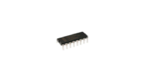
Figure 1: 74HC595
The 74HC595 is an 8-bit shift register that combines serial input with parallel output, offering unique tri-state output options. This complex component operates by receiving serial data through its serial data input (SDI) on the rising edge of the serial clock (SCK). The internal 8-bit shift register processes the data, sequentially outputting from the Q7' terminal—the highest point of serial data output.
- Serial Clock (SCK): Triggered on the rising edge
- Serial Data Input (SDI): Receives 8-bit data
- Q7' Terminal: Highest bit serial data output
- The conversion to parallel output unfolds on the rising edge of the latch control (LCK). It is at this moment that the data in the 8-bit shift register is locked into the 8-bit parallel output register. The values exposed by the parallel outputs are the same as those stored in them, depending on the output enable (OE) signal being low (enabled).
- Latch Control (LCK): Activated on the rising edge
- Output Enable (OE): Activated when low
Alternatives and Equivalent Options
Pin Configuration and Functions
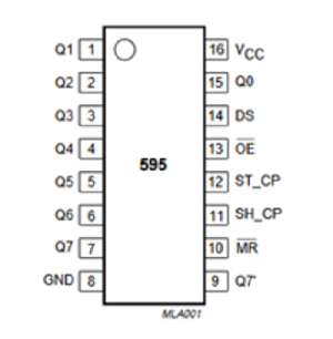
Figure 2: 74HC595 Pinout
The 74HC595 has 16 pins, whose layout proves its versatility:
SER (Pin 1): The gateway for serial data, SER pin, helps in bit-by-bit transmission into the chip. It initiates data transfer in parallel, one clock pulse at a time.
RCLK (Pin 2): Acting as the register clock input, RCLK oversees the movement of data from the shift register to the output register, ensuring synchronized data storage.
SRCLK (Pin 3): This shift register clock input pin coordinates shift operations, managing the pace of data conversion.
OE (Pin 4): The output enable input indicates data transfer through output pins, switching between enabled and disabled states via its voltage level.
DS (Pin 5): A bidirectional serial data input, DS provides an alternative data entry point, enhancing communication flexibility.
ST_CP (Pin 6): Output store trigger clock input controls the timing of data storage in output pins, reflecting changes in the store trigger clock signal.
SH_CP (Pin 7): Controls the clock input of the shift register, SH_CP is crucial for migrating data in sequence to the shift register.
Q7' (Pin 8) to Q0-Q7 (Pins 9-16): These output pins represent the core of parallel data propagation, echoing the data of the shift register from the lowest to the highest bit.
Logic Diagram of 74HC595
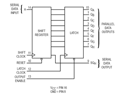
Figure 3: 74HC595 Logic Diagram
Applications of 74HC595
The 74HC595 excels in multiple areas, showcasing its adaptability and efficiency:
Relay Control: Its parallel output functionality allows for simultaneous control of multiple relays, each capable of manipulating one or more electrical devices. This enables the creation of dynamic and robust electrical control systems.
Digital Output Expansion: By connecting a microcontroller's output pins to the 74HC595's serial input, output ports can be conveniently expanded, thereby extending control over other devices.
Display Control: In LCD control scenarios, the 74HC595 smoothly transfers display data to the screen using its serial-to-parallel conversion, ensuring seamless updates of text, images, or video.
Music Beat Lights: Integrating beat control algorithms with the 74HC595 can create LED effects perfectly synchronized with the music rhythm. This fusion captures the essence of music beats, transforming them into captivating LED displays of various frequencies, brightness, and colors.
Use Cases of 74HC595
Designing a Multi-Digit LED Display Using 74HC595
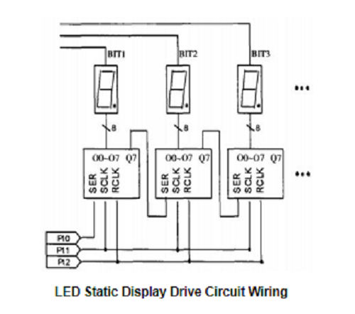
Figure 4: Multi-bit LED display design based on 74HC595
Static Display Method
In the realm of static displays, each LED segment selection line is intricately connected to the parallel outputs of the 74HC595. This connection scheme allows each digit to display independently, with character changes directly managed by the outputs of individual 74HC595 chips.
Parallel Outputs: Each 74HC595 controls a digit.
Character Changes: The display can show different characters.
Although resource-intensive, requiring N 74HC595 chips and N+3 I/O lines for an N-digit LED display, this method also highlights the complexity and cost implications associated with multi-digit LED displays.
Dynamic Display Method
To simplify circuit design, reduce costs, and save system resources for multi-digit LED displays, a unified approach is adopted. Here, the segment codes of all digits are parallelly and managed by a single 74HC595 chip.
Unified Control: A single 74HC595 controls all digit segments.
Scanning Method: Characters are displayed sequentially on LEDs.
Using scanning technology, only one LED character is displayed at any given moment, cycling through each digit to present the intended characters. The latch function of the 74HC595 eliminates the need for additional delays, facilitating a persistence of vision effect without sacrificing operational speed.
LED Drive Circuit Design Using the 74HC595 Chip
The 74HC595 chip is a member of the 74 series, known for its fast operation, low power consumption, and ease of use. It serves as an effective bridge between microcontrollers and LED displays, offering many advantages.
LED Displays
LED displays, especially seven-segment LED displays, are favored for their cost-effectiveness, low power consumption, and reliability. While feature-rich dedicated LED drivers are available, their higher cost makes the 74HC595 a preferred choice for budget-conscious and simplified systems.
Advantages of Using 74HC595: Fast speed, low power consumption, capable of driving different numbers of LEDs.
Flexibility and Power Efficiency: The 74HC595 enables easy brightness control and energy-saving operations, suitable for both common anode and common cathode displays.
Design Using the 74HC595 Chip
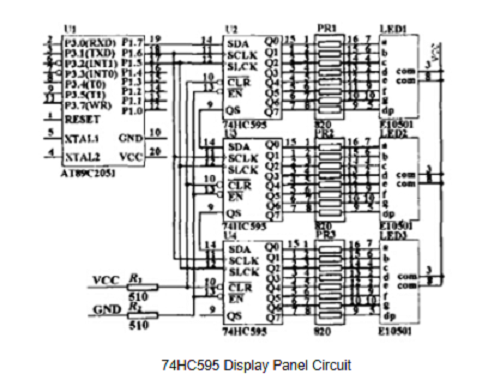
Figure 5: Designed with 74HC595 chip
This setup is illustrated through an interface design with the AT89C2051 microcontroller and the 74HC595, showcasing a voltage display using three digital tubes, emphasizing the importance of orderly data presentation and adjustable brightness.
Control Pins (P115, P116, P117): Manage the brightness and sequence of LED displays.
Enhancing the Driving Capability of the 74HC595
Buffers or Drivers: Using buffers like the 74LS244 (unidirectional) or 74LS245 (bidirectional) can enhance signal driving strength and stability.
Appropriate Power Supply: Ensuring the power supply is within the recommended voltage range and has sufficient power to meet load requirements is crucial for optimal performance.
External Drive Circuits: For loads exceeding the direct output capability of the 74HC595, external drive circuits using transistors, FETs, or dedicated driver chips can amplify the output signal.
PCB Layout Considerations: Minimizing resistance and inductance in PCB traces can improve signal transmission efficiency while avoiding excessive noise and interference to maintain signal quality.
Suitable Load Resistors: Choosing load resistors based
on the characteristics of the load device can prevent overcurrent situations that could damage the 74HC595 chip.
Parallel Output Configuration: For applications requiring a large number of devices with similar driving requirements, paralleling the outputs of multiple 74HC595 chips can enhance overall driving capability, provided the combined current does not exceed the chip's maximum output limit.
Frequently Asked Questions [FAQ]
1. Is the 74HC595 a microcontroller?
The 74HC595 is a shift register operating on a Serial IN Parallel OUT protocol. It receives data serially from a microcontroller and then sends that data through parallel pins.
2. What is the function of the 74HC595?
The 74HC595 is a high-speed CMOS device. The eight-bit shift register accepts data from the serial input (DS) with each positive transition of the shift register clock (SHCP). When set to low, the reset function sets all shift register values to zero independently of all clocks.
3. How much current can the 74HC595 withstand?
The datasheet for the 74HC595 states that each output can provide at least 35mA of current, as this is the maximum allowed output current. This clearly exceeds the 25mA allowed by µC. Another limitation is the total amount of current provided by the 74HC595 should not exceed 70mA.
4. What is the difference between MAX7219 and 74HC595?
The 74HC595 is a shift register, while the MAX7219 is a multiplexed display driver. Thus, they do not do the same thing. If using a multiplexed display, the MAX7219 would be (more) easy to use with PICAXE, as the task of multiplexing the display is done by the MAX7219 and not the PICAXE, but it is more expensive.
About us
ALLELCO LIMITED
Read more
Quick inquiry
Please send an inquiry, we will respond immediately.
The Function and Working Principle of BTN8982TA
on March 15th

Crossover vs. straight-through cable selection guide - differences, wiring styles, how to choose
on March 12th
Popular Posts
-
What is GND in the circuit?
on January 1th 3272
-

RJ-45 Connector Guide: RJ-45 Connector Color Codes, Wiring Schemes, R-J45 Applications, RJ-45 Datasheets
on January 1th 2815
-
Understanding Power Supply Voltages in Electronics VCC, VDD, VEE, VSS, and GND
on November 20th 2642
-

Fiber Connector Types: SC Vs LC And LC Vs MTP
on January 1th 2265
-

Comparison Between DB9 and RS232
on January 1th 1882
-

What Is An LR44 Battery?
Electricity, that ubiquitous force, quietly permeates every aspect of our daily lives, from trivial gadgets to life-threatening medical equipment, it plays a silent role. However, truly grasping this energy, especially how to store and efficiently output it, is no easy task. It is against this background that this article will focus on a type of coin cell battery that may seem insignificant on the...on January 1th 1846
-
Understanding the Fundamentals:Inductance Resistance, andCapacitance
In the intricate dance of electrical engineering, a trio of fundamental elements takes center stage: inductance, resistance, and capacitance. Each bears unique traits that dictate the dynamic rhythms of electronic circuits. Here, we embark on a journey to decipher the complexities of these components, to uncover their distinct roles and practical uses within the vast electrical orchestra. Inductan...on January 1th 1808
-
What Is RF and Why Do We Use It?
Radio Frequency (RF) technology is a key part of modern wireless communication, enabling data transmission over long distances without physical connections. This article delves into the basics of RF, explaining how electromagnetic radiation (EMR) makes RF communication possible. We will explore the principles of EMR, the creation and control of RF signals, and their wide-ranging uses. The article ...on January 1th 1801
-
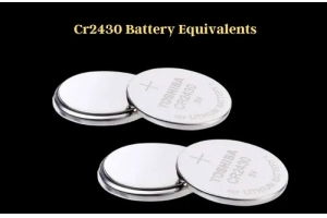
CR2430 Battery Comprehensive Guide: Specifications, Applications and Comparison to CR2032 Batteries
What is CR2430 battery ?Benefits of CR2430 BatteriesNormCR2430 Battery ApplicationsCR2430 EquivalentCR2430 VS CR2032Battery CR2430 SizeWhat to look for when buying the CR2430 and equivalentsData Sheet PDFFrequently Asked Questions Batteries are the heart of small electronic devices. Among the many types available, coin cells play a crucial role, commonly found in calculators, remote controls, and ...on January 1th 1799
-
Comprehensive guide to hFE in transistors
Transistors are crucial components in modern electronic devices, enabling signal amplification and control. This article delves into the knowledge surrounding hFE, including how to select a transistor's hFE value, how to find hFE, and the gain of different types of transistors. Through our exploration of hFE, we gain a deeper understanding of how transistors work and their role in electronic circu...on November 20th 1782
HOT Part Number
-
STD11NM60N
STMicroelectronics
MOSFET N-CH 600V 10A DPAK
PS2561DL-1Y-F3-A
Renesas Electronics America Inc
OPTOISOLATOR 5KV TRANS 4SMD
CL31B224KACNFNC
Samsung Electro-Mechanics
CAP CER 0.22UF 25V X7R 1206
OPA1671IDCKT
Texas Instruments
IC AUDIO 1 CIRCUIT SC70-5
P1500SARP
Littelfuse Inc.
THYRISTOR 140V 150A DO214AA
MIC5504-2.8YMT-TZ
Microchip Technology
IC REG LINEAR 2.8V 300MA 4TDFN
SN74CBTLV3245APWR
Texas Instruments
IC BUS SWITCH 8 X 1:1 20TSSOP
GCM1885C2A2R2CA16J
Murata Electronics
CAP CER 2.2PF 100V C0G/NP0 0603
PEB24911HV1.3
Infineon Technologies
ISDN ECHOCANCELLER DFE
SN75ALS173NSR
Texas Instruments
IC RECEIVER 0/4 16SO
MAX15007AASA+T
Analog Devices Inc./Maxim Integrated
IC REG LINEAR 3.3V 50MA 8SOIC
SN74LS257BD
Motorola
74LS257B - QUADRUPLE 2-LINE TO 1
H1081NLT
Pulse Electronics
XFRMR MODUL 1PORT 1:1.141 10/100
MKL24Z64VFT4
NXP USA Inc.
IC MCU 32BIT 64KB FLASH 48QFN
GRM1555C1E2R8BA01D
Murata Electronics
CAP CER 2.8PF 25V C0G/NP0 0402
GRM2196T2A6R3DD01D
Murata Electronics
CAP CER 6.3PF 100V T2H 0805
P6KE220A
Diotec Semiconductor
TVS DO-15 185V 600W UNI
SN75453BDRG4
Texas Instruments
IC PERIPHERAL DRIVER 5.25V 8SOIC -
LM4140BCM-2.0
Texas Instruments
IC VREF SERIES 0.1% 8SOIC
GRM0335C1E3R9CA01J
Murata Electronics
CAP CER 3.9PF 25V C0G/NP0 0201
VSC8115XYA-05-T
Microchip Technology
IC CLK DATA REC SDH 622MBPS
GRM1886P1H6R5DZ01D
Murata Electronics
CAP CER 6.5PF 50V P2H 0603
IRF1404ZSTRLPBF
Infineon Technologies
MOSFET N-CH 40V 180A D2PAK
ZM4733A-GS08
Vishay General Semiconductor - Diodes Division
DIODE ZENER 5.1V 1W DO213AB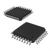
8735BYI-01LFT
Renesas Electronics America Inc
IC CLK GEN LVPECL ZD 1:5 32LQFP
MC74LCX74DT
onsemi
IC FF D-TYPE DUAL 1BIT 14TSSOP
AD8191ASTZ
Analog Devices Inc.
IC VIDEO SWITCH 100LQFP
M81706AFP
Powerex Inc.
IC HALF BRIDGE DRIVER 8SOP
MC74VHC1GT04DFT2
onsemi
IC GATE INVERTER SNGL 1IN SOT353
XC95108-20PQ100C
AMD
IC CPLD 108MC 20NS 100QFP
ISL8036IRZ-T
Renesas Electronics America Inc
IC REG BUCK ADJ 3A SGL/DL 24QFN
ES3GBF
Yangjie Technology
Diodes - Rectifiers - Single SMB
OPA2314AIDRBT
Texas Instruments
IC CMOS 2 CIRCUIT 8SON
PM105SB-150M-RC
Bourns Inc.
FIXED IND 15UH 1.7A 70 MOHM SMD
MT40A256M16LY-075:F
Micron Technology Inc.
DDR4 4G 256MX16 FBGA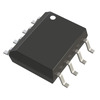
LT1763CS8#PBF
Analog Devices Inc.
IC REG LINEAR POS ADJ 500MA 8SO -

SP6260EEK-L/TR
MaxLinear, Inc.
IC REG LINEAR 3V 200MA SOT23-5
LT1242IS8#PBF
Analog Devices Inc.
IC OFFLINE SWITCH BUCK 8SOIC
C50P
Powerex Inc.
SCR 1000V 70A TO94
ZXMN10A25K
Diodes Incorporated
MOSFET N-CH 100V 4.2A TO252-3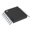
SN74CBT3253CDBR
Texas Instruments
IC MUX/DEMUX 2 X 4:1 16SSOP
ATMEGA329-16MI
Microchip Technology
IC MCU 8BIT 32KB FLASH 64QFN
SI8404DB-T1-E1
Vishay Siliconix
MOSFET N-CH 8V 12.2A 4MICROFOOT
08053A102JA12A
KYOCERA AVX
CAP CER 1000PF 25V NP0 0805
CY8CTMA395-LTI-00
Cypress Semiconductor Corp
TRUE TOUCH MCU
CY7C1460KV33-200AXC
Infineon Technologies
IC SRAM 36MBIT PARALLEL 100TQFP
HI20201JCB
Intersil
IC DAC 10BIT A-OUT 28SOIC
HLMP-D150
Broadcom Limited
LED RED DIFFUSED T-1 3/4 T/H
MAX187BCWE+T
Analog Devices Inc./Maxim Integrated
IC ADC 12BIT SAR 16SOIC
CRCW08051K00FKEA
Vishay Dale
RES SMD 1K OHM 1% 1/8W 0805
INA821IDGKR
Texas Instruments
IC INST AMP 1 CIRCUIT 8VSSOP
PI3V512QE
Diodes Incorporated
IC SWITCH 2:1 5 PORT 24QSOP
1N3348RB
Microchip Technology
DIODE ZENER 220V 50W DO5
TPS25940AQRVCRQ1
Texas Instruments
IC ELECTRONIC FUSE 8% 20WQFN