74HC132 Trigger: Datasheet, Alternatives, and Pinout
This article takes a look at the 74HC132, a simple yet powerful electronic part called a two-input NAND Schmitt Trigger Gate. Built with modern C²MOS technology, this little chip is known for switching quickly, saving power, and fitting well into different circuits. It’s a small but impressive example of how technology keeps moving forward. The 74HC132 is used in all kinds of electronic devices, showing just how important it is in today’s world of electronics. In this article, we’ll break down how it works, what makes it special, and where you’ll find it in applications.Catalog
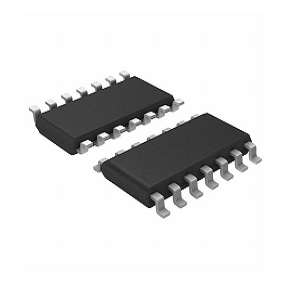
What is the 74HC132?
The 74HC132 represents a high-speed, low-power 2-input NAND Schmitt Trigger gate, crafted with advanced C²MOS technology. This component is engineered to merge the quick operations akin to LSTTL chips with the energy-conserving benefits native to CMOS technology. This seamless integration allows the device to perform admirably across a variety of computing settings, enhancing its appeal for contemporary electronic applications. One remarkable aspect of the 74HC132 is its proficiency in managing slow input signals efficiently, assisted by a 25% VCC hysteresis at its inputs. This trait aids in mitigating noise, in high-precision tasks where signal integrity is needed. In signal processing environments, where slow or variable signals can provoke challenges, the 74HC132 exudes resilience against potential disruptions, ensuring dependable performance.
The 74HC132 encompasses robust safeguards against static discharge and transient voltage spikes, contributing to increased durability and reliability. Reflecting on industrial scenarios, systems that incorporate sophisticated protection strategies tend to exhibit enduring robustness, showcasing the importance of these features in practical applications. The combination of rapid speed and reduced power consumption within a single component, exemplified by the 74HC132, becomes notable amidst rising demands for energy-efficient designs. The tangible benefits observed in sustainability-focused industries underscore the merit of achieving such efficiency. Incorporating low-power elements in large-scale deployments can dramatically cut down overall energy usage, yielding substantial long-term economic advantages.
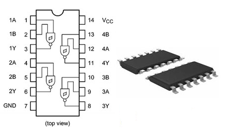
74HC132 Pin Configuration
|
Pin Number |
Pin Name |
Description |
|
1 |
1A |
Channel 1, Input A |
|
2 |
1B |
Channel 1, Input B |
|
3 |
1Y |
Channel 1, Output Y |
|
4 |
2A |
Channel 2, Input A |
|
5 |
2B |
Channel 2, Input B |
|
6 |
2Y |
Channel 2, Output Y |
|
7 |
GND |
Ground |
|
8 |
3Y |
Channel 3, Output Y |
|
9 |
3A |
Channel 3, Input A |
|
10 |
3B |
Channel 3, Input B |
|
11 |
4Y |
Channel 4, Output Y |
|
12 |
4A |
Channel 4, Input A |
|
13 |
4B |
Channel 4, Input B |
|
14 |
VCC |
Positive Supply |
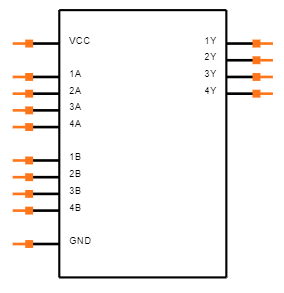
74HC132 Symbol, Footprint, and CAD Model
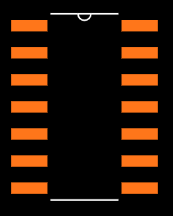
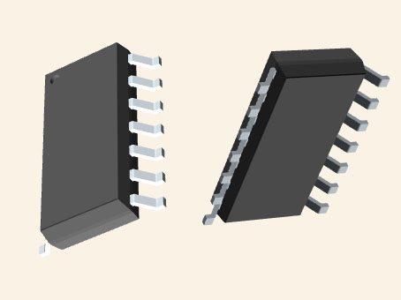
Features of 74HC132
High-Speed Operation
The 74HC132 delivers remarkable performance with its swift speed, featuring a propagation delay of merely 11 ns at 5V. This speed facilitates rapid data handling and provides an edge in scenarios demanding quick logic decisions. Others harness this capability to improve circuit performance in digital communication systems where efficiency is needed.
Energy Use
Exhibiting minimal energy draw, topping at just 1.0 µA at 25°C, the 74HC132 suits applications sensitive to energy consumption. This low power usage, coupled with its strong functionality, supports designs focused on sustainability, contributing to energy conservation in both portable devices and fixed installations. Many find this aspect for constructing economically and environmentally friendly devices.
Reliability in Noisy Environments and Voltage Flexibility
The 74HC132 is noteworthy for its high noise immunity, providing stable functionality even amidst electrical interference. Its support for a voltage range spanning from 2.0V to 6.0V enhances its compatibility across various power conditions. These characteristics are often leveraged to ensure data integrity and consistent device performance under diverse operational settings.
Adaptability and Compliance with Industry Standards
By aligning with JEDEC standards, the 74HC132 ensures seamless compatibility and interoperability within electronic systems. Protection against ESD (Electrostatic Discharge) and latch-up enhances its use across a wide range of sectors, including automotive, industrial, and electronics. Its adherence to industry norms frequently makes it a preferred choice in design scenarios.
74HC132 Technical Specifications
Technical specifications, characteristics, parameters, and compatible components for Toshiba Semiconductor and Storage's 74HC132, similar to the 74HC132D.
|
Type |
Parameter |
|
Factory Lead Time |
12 Weeks |
|
Package / Case |
14-SOIC (0.154, 3.90mm Width) |
|
Usage Level |
Industrial grade |
|
Packaging |
Cut Tape (CT) |
|
Published |
2016 |
|
Moisture Sensitivity Level (MSL) |
1 (Unlimited) |
|
Voltage - Supply |
2V~6V |
|
Terminal Form |
GULL WING |
|
Number of Functions |
4 |
|
Time@Peak Reflow Temperature-Max (s) |
NOT SPECIFIED |
|
Supply Voltage-Min (Vsup) |
2V |
|
Family |
HC/UH |
|
Logic Type |
NAND Gate |
|
Current - Quiescent (Max) |
1µA |
|
Length |
8.85mm |
|
Width |
3.9mm |
|
Mounting Type |
Surface Mount |
|
Surface Mount |
YES |
|
Operating Temperature |
-40°C~85°C |
|
Series |
74HC |
|
Part Status |
Active |
|
Number of Terminations |
14 |
|
Terminal Position |
DUAL |
|
Peak Reflow Temperature (Cel) |
NOT SPECIFIED |
|
Supply Voltage |
5V |
|
Supply Voltage-Max (Vsup) |
6V |
|
Number of Circuits |
4 |
|
Number of Inputs |
2 |
|
Max Propagation Delay @ V, Max CL |
19ns @ 5V, 50pF |
|
Features |
Schmitt Trigger |
|
Height Seated (Max) |
1.75mm |
|
RoHS Status |
RoHS Compliant |
Voltage Doubling with 74HC132
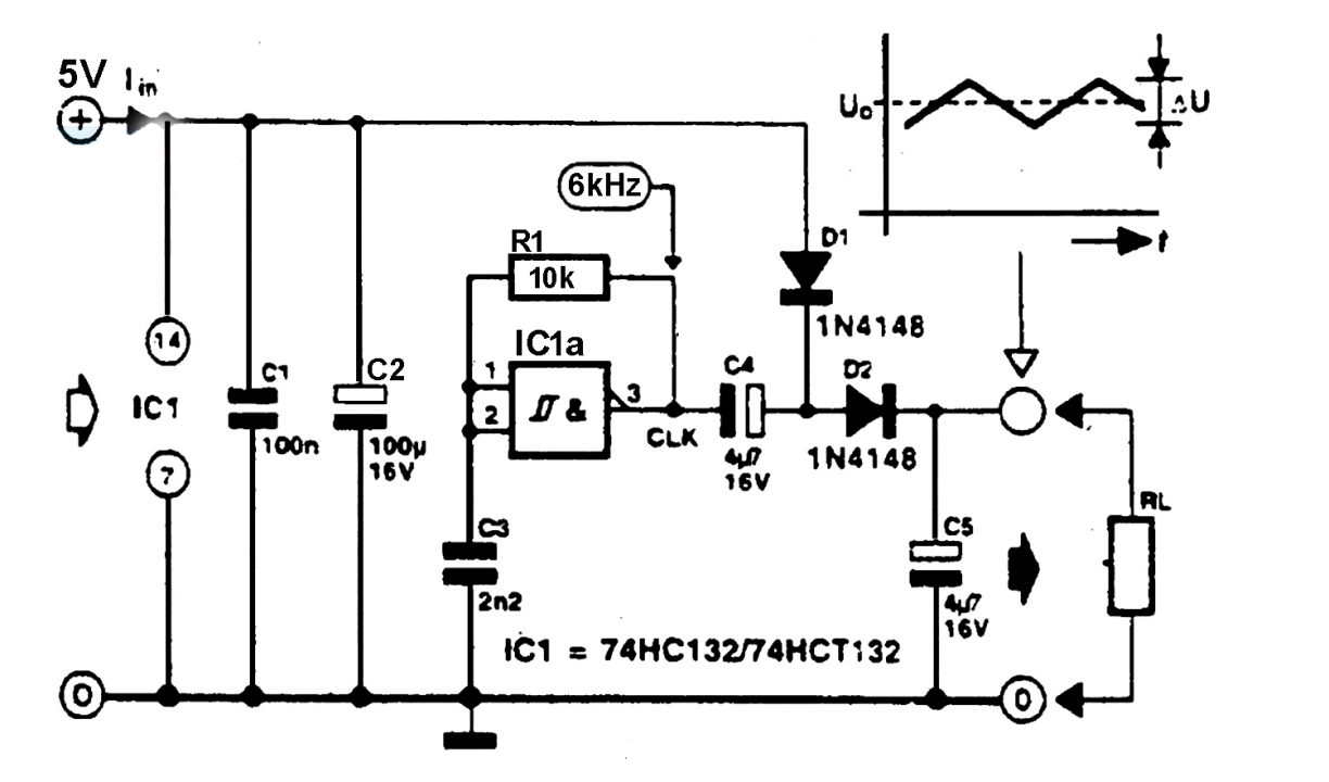
The 74HC132 quad NAND Schmitt trigger serves as a flexible foundation for creating a robust circuit designed to boost voltage efficiently. By integrating elements such as capacitors and diodes, this circuit can elevate a 5V input to nearly 10V. The design's straightforwardness not only reduces cost in voltage conversion tasks but also demonstrates its practical use across a range of power management applications. With a deep dive into the intricacies of choosing capacitors and understanding diode properties, you can enhance the voltage output's efficiency and steadiness.
In designing a voltage doubler circuit, selecting appropriate capacitors and diodes plays a role. Opting for capacitors with low equivalent series resistance (ESR) reduces energy loss, enhancing efficiency. Diodes with minimal forward voltage drop are good for amplifying voltage effectively. These thoughtful decisions greatly shape the circuit's functionality, aiding in achieving favorable results in their electronic creations.
Implementing capacitors and diodes in voltage doubling is not limited to their technical features alone. For example, the use of tantalum capacitors can offer resilience in unstable temperature conditions. Schottky diodes, favored for their lower forward voltage drop, are often chosen for similar reasons. Creating a voltage doubler involves more than just picking parts; it demands careful attention to circuit design and timing regulation via the 74HC132. Refining the setup can improve the circuit's efficiency and dependability. This rigorous process mixes theoretical understanding with practical experimentation, where continuous improvements refine the circuit's performance over time.
Alternatives to the 74HC132
|
Part Number |
Description |
Manufacturer |
|
74HC132PW |
NAND Gate, HC/UH Series, 4-Func, 2-Input, CMOS, PDSO14 |
Nexperia |
|
74HC132PW-T |
IC HC/UH SERIES, QUAD 2-INPUT NAND GATE, PDSO14,
SOT-402-1, TSSOP-14, Gate |
NXP Semiconductors |
|
MC74HC132ADTR2G |
Quad 2-Input NAND Gate with Schmitt Trigger Input,
TSSOP-14, 2500-REEL |
onsemi |
Applications for 74HC132
Adaptive Applications in Signal Shaping
The 74HC132 serves the unique purpose of crafting wave and pulse shapers, elements that play a role in modern electronics. These waveforms are good for molding digital signals across various applications, maintaining integrity and accuracy. Many driven by challenges in waveform generation, find that the predictability and stability offered by the 74HC132 greatly aid in refining signal parameters.
Deployment in Astable Multivibrators
In designing astable multivibrators, the 74HC132 becomes a highly useful component, enhancing applications that require uninterrupted square wave generation. The iterative process of experimentation reveals that this component's consistent reliability and output frequency stability. A wide frequency range is achievable by skillfully adjusting the resistance-capacitance network, a fact that resonates with those deeply familiar with circuit design.
Crafting Monostable Multivibrators
Within monostable multivibrators, the 74HC132 functions as a building block, transforming input triggers into single output pulses. Efficiency is heightened as employ the 74HC132, capitalizing on its ability to yield consistent pulse durations. Sensitive to input variations, appreciate its contribution to precision when timing is of the essence.
Advancing Timing Signal Generation
The ability of the 74HC132 to generate timing signals highlights its relevance in a variety of electronic situations. As circuit complexity increases, there is a growing need for reliable timing solutions. The dependable timing outputs of the 74HC132, achieved through careful configuration, speak to its effectiveness. The 74HC132 is distinguished by its flexibility and efficiency across multiple electronic applications, meeting the dynamic needs of technology with ease and ensuring seamless operations and superior signal quality.
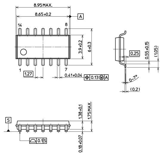
Package of 74HC132
74HC132 Manufacturer Information
Toshiba Semiconductor & Storage deeply influences the development of integrated products across multiple sectors, with a focus on automotive and digital markets. These fields' rapidly changing technological landscapes invite creativity and forward-thinking, embodying the qualities Toshiba seeks to instill. A fascinating aspect of Toshiba's influence in semiconductor and storage technology is its ability to impact global market trends. As the progression of technological innovation unfolds, Toshiba's efforts might act as a catalyst for future developments in electronics and automotive technologies. This foresight inspires industry stakeholders to view strategic alliances and innovation-focused growth as important aspects of future achievements.
Datasheet PDF
74HC132D Datasheets:
MC74HC132ADTR2G Datasheets:
Material Declaration MC74HC132ADTR2G.pdf
Assembly Change 16/Feb/2023.pdf
About us
ALLELCO LIMITED
Read more
Quick inquiry
Please send an inquiry, we will respond immediately.
Frequently Asked Questions [FAQ]
1. What chip is 74HC132?
The 74HC132 is a quad 2-input NAND gate that operates seamlessly within a 2V to 6V voltage range. Unlike the Schmitt trigger variant, this model provides a different set of capabilities, allowing it to handle specific operational requirements.
2. If the motherboard power-on circuit is broken, what type of replacement should be used for 74HC132?
To address a malfunctioning 74HC132 on a motherboard, consider alternatives like the 74HCT132D or 74AHC132D. It's need to verify that the new component matches the voltage and logic parameters of the existing setup. By choosing an appropriate substitute, you enhance the system’s durability, mirroring standard practices where component compatibility is good for preserving system functionality.
3. What is the role of 74HC132?
The 74HC132 is proficient in executing NAND operations, with the Schmitt-triggered input feature adding to its capability by improving signal stability and immunity to noise. This is pertinent in environments prone to electrical interference, where maintaining signal integrity is good for ensuring satisfactory operation. Such integration aligns with techniques in telecommunications, prioritizing robustness to safeguard signal clarity amidst potential disturbances.
Understanding the STM32F411CEU6
on November 7th
Comprehensive Guide to BTA16 Triacs: Features, Pinout, and Datasheet
on November 7th
Popular Posts
-
What is GND in the circuit?
on January 1th 3040
-

RJ-45 Connector Guide: RJ-45 Connector Color Codes, Wiring Schemes, R-J45 Applications, RJ-45 Datasheets
on January 1th 2609
-

Fiber Connector Types: SC Vs LC And LC Vs MTP
on January 1th 2162
-
Understanding Power Supply Voltages in Electronics VCC, VDD, VEE, VSS, and GND
on November 13th 2077
-

Comparison Between DB9 and RS232
on January 1th 1790
-

What Is An LR44 Battery?
Electricity, that ubiquitous force, quietly permeates every aspect of our daily lives, from trivial gadgets to life-threatening medical equipment, it plays a silent role. However, truly grasping this energy, especially how to store and efficiently output it, is no easy task. It is against this background that this article will focus on a type of coin cell battery that may seem insignificant on the...on January 1th 1754
-
Understanding the Fundamentals:Inductance Resistance, andCapacitance
In the intricate dance of electrical engineering, a trio of fundamental elements takes center stage: inductance, resistance, and capacitance. Each bears unique traits that dictate the dynamic rhythms of electronic circuits. Here, we embark on a journey to decipher the complexities of these components, to uncover their distinct roles and practical uses within the vast electrical orchestra. Inductan...on January 1th 1706
-

CR2430 Battery Comprehensive Guide: Specifications, Applications and Comparison to CR2032 Batteries
What is CR2430 battery ?Benefits of CR2430 BatteriesNormCR2430 Battery ApplicationsCR2430 EquivalentCR2430 VS CR2032Battery CR2430 SizeWhat to look for when buying the CR2430 and equivalentsData Sheet PDFFrequently Asked Questions Batteries are the heart of small electronic devices. Among the many types available, coin cells play a crucial role, commonly found in calculators, remote controls, and ...on January 1th 1642
-
What Is RF and Why Do We Use It?
Radio Frequency (RF) technology is a key part of modern wireless communication, enabling data transmission over long distances without physical connections. This article delves into the basics of RF, explaining how electromagnetic radiation (EMR) makes RF communication possible. We will explore the principles of EMR, the creation and control of RF signals, and their wide-ranging uses. The article ...on January 1th 1623
-
Comprehensive guide to hFE in transistors
Transistors are crucial components in modern electronic devices, enabling signal amplification and control. This article delves into the knowledge surrounding hFE, including how to select a transistor's hFE value, how to find hFE, and the gain of different types of transistors. Through our exploration of hFE, we gain a deeper understanding of how transistors work and their role in electronic circu...on November 13th 1566
