TPS5430 In-Depth Overview: High Efficiency PWM Converter
Catalog
TPS5430 Description
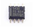
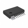
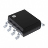
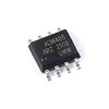
The TPS5430 is a high output current PWM converter that integrates a low resistance, high-side N-channel MOSFET. This converter offers a range of outstanding features, including a high-performance voltage error amplifier that provides high regulation accuracy under transient conditions; undervoltage lockout circuitry to prevent startup when the input voltage does not reach 5.5V; internally set A slow-start circuit to limit inrush current and a voltage feed-forward circuit to improve transient response. By using the ENA pin, the shutdown supply current can be reduced to typically 15µA. In addition, TPS5430 also has features such as high-level active enable terminal, over-current limit, over-voltage protection and thermal shutdown. To simplify design and reduce external component count, the TPS5430's feedback loop has been internally compensated. At the same time, the TPS5430 can regulate a variety of power supplies, including the 24V bus, allowing it to perform excellently in various application scenarios. In addition, the TPS5430 is available in a thermally enhanced, easy-to-use 8-pin SOIC PowerPAD integrated circuit package. To help users quickly implement high-performance power supply designs and meet tight device development cycle needs, TI also provides evaluation modules and designer software tools. These tools will help users design power supplies more effectively and improve work efficiency.
Alternatives and equivalents:
• LM22673
• LM22676
• RT2808A
• TPS5420
Pin Arrangement and Description of TPS5430
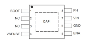
As shown in the picture above, TPS5430 has eight pins, their names and descriptions are as follows:
Pin 1 (BOOT): Boost capacitor for the high-side FET gate driver. Connect 0.01μF low ESR capacitor from BOOT pin to PH pin.
Pin 2~3 (NC): Not connected internally.
Pin 4 (VSENSE): Feedback voltage for the regulator. Connect to output voltage divider.
Pin 5 (ENA): On and off control. Below 0.5V, the device stops switching. Float the pin to enable.
Pin 6 (GND): Ground. Connect to DAP.
Pin 7 (VIN): Input supply voltage. Bypass VIN pin to GND pin close to device package with a high quality, low ESR ceramic capacitor.
Pin 8 (PH): Source of the high side power MOSFET. Connected to external inductor and diode.
Characteristics of TPS5430
TPS5430 usually has the following characteristics:
Low power consumption: TPS5430 has multiple working modes, which can automatically adjust the operating frequency and current according to the actual load conditions, thereby achieving low power consumption operation. Under light load or no-load conditions, the TPS5430 can enter sleep mode, greatly reducing power consumption.
High efficiency: TPS5430 adopts advanced switching control technology, making the power conversion efficiency as high as 96 percent. In practical applications, it can effectively reduce power loss and improve the overall performance of the device.
Good thermal performance: TPS5430 adopts an advanced heat dissipation design, which can effectively conduct heat to the radiator to ensure stable operation of the device in high temperature environments.
High conversion efficiency: In practical applications, TPS5430 can efficiently convert input power into output power, greatly reducing energy loss and thus improving the overall performance of the device. This efficient conversion not only helps reduce system energy consumption, but also reduces heat dissipation issues and improves system stability and reliability.
High integration: TPS5430 integrates a variety of functional modules, including overvoltage protection, current limit, voltage conversion, undervoltage protection, etc., which greatly reduces the design complexity of peripheral circuits. At the same time, the TPS5430 adopts a small package to facilitate integration into various electronic devices.
Functional Modes of TPS5430
Operation with ENA Control
The enable start threshold voltage is 1.3 V max. With ENA held below the 0.5 V minimum stop threshold voltage, the TPS5430 is disabled and switching is inhibited even if VIN is above its UVLO threshold. The quiescent current is reduced in this state. If the ENA voltage is increased above the max start threshold while V(VIN) is above the UVLO threshold, the device becomes active. Switching is enabled and the slow-start sequence is initiated. The TPS5430 starts linearly ramping up the internal reference voltage from 0 V to its final value over the internal slow-start time period.
Operation Near Minimum Input Voltage
The TPS5430 is recommended to operate with input voltages above 5.5 V. The typical VIN UVLO threshold is 5.3 V and the device can operate at input voltages down to the UVLO voltage. At input voltages below the actual UVLO voltage the device will not switch. If EN is floating or externally pulled up to greater up than 1.3 V, when V(VIN) passes the UVLO threshold the TPS5430 will become active. Switching is enabled and the slow-start sequence is initiated. The TPS5430 starts linear ramping up the internal reference voltage from 0 V to its final value over the internal slow-start time period.
What Are the Advantages and Disadvantages of TPS5430?
Advantages of TPS5430
Compact package: TPS5430 adopts a compact package form, usually an 8-pin SOP or MSOP package, which is small and suitable for use in application scenarios with limited space.
Protection functions: TPS5430 has a variety of built-in protection functions, including overload protection, overheat protection, undervoltage lockout protection, etc., which can improve the stability and reliability of the system, as well as protect the load and the IC itself from damage.
Wide input voltage range: The TPS5430 is able to adapt to a wide range of input voltages, operating from 3.5V to 28V. This makes it suitable for a variety of different power supply input conditions, providing greater flexibility.
Adjustable output: The TPS5430 features adjustable output voltage and current limit. Users can adjust the output voltage to meet specific needs and can set current limits to protect the load.
High efficiency performance: The TPS5430 is a high efficiency DC-DC buck converter that utilizes advanced switching regulation technology to provide a stable output voltage at up to 95 percent efficiency. This feature enables the TPS5430 to operate with significantly less energy waste and system heat generation.
Disadvantages of TPS5430
Higher cost: Compared with some traditional linear regulators, the cost of the TPS5430 may be on the high side, which can be a limiting factor in some cost-sensitive applications.
Electromagnetic interference: As a switching regulator, the TPS5430 may generate some electromagnetic interference during operation, requiring appropriate shielding and filtering measures to avoid interference with surrounding circuits.
Complexity: The advanced functions and complex circuit design of TPS5430 may require users to have certain technical knowledge and experience. Therefore, it may be challenging for beginners to learn and master its use.
Application of TPS5430 in Earthquake Precursor Observation Data Acquisition System
The data acquisition system is an important part of the earthquake precursor observation instrument. It converts the weak analog signals detected by the sensors into digital signals and performs calculations to provide reliable data for subsequent earthquake analysis.
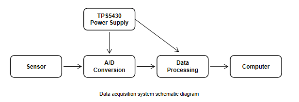
Initially, we used chip power supplies such as MAX1626 to power the TJ-2 volumetric strain gauge data acquisition system, but during the test we found that the system was unstable and the instrument would automatically restart. The reason was found to be that the load capacity of the power supply of MAX1626 and other chips was not large enough. Therefore, after many investigations, we finally selected the TPS5430 chip, which has strong load capacity, high efficiency, and few peripheral components, as the power supply to power the A/D conversion module and data processing module of the data acquisition system. The principle is as follows.
How Does TPS5430 Achieve Low Power Consumption and High Efficiency Power Conversion?
First of all, TPS5430 uses advanced switching control technology, which can significantly improve power conversion efficiency, up to 96 percent. In practical applications, this high-efficiency power conversion can effectively reduce power losses and improve the overall performance of the device. Secondly, the TPS5430 has multiple working modes, which can automatically adjust the operating frequency and current according to the actual load conditions, thereby achieving low-power operation. Under light load or no-load conditions, the TPS5430 can enter sleep mode to further reduce power consumption. The switching of these working modes is automatic without manual intervention, thus ensuring the efficiency and stability of power conversion. In addition, TPS5430 also features fast dynamic response and high-precision output voltage. This is due to its current mode control technology and Texas Instruments' D-CAP2 architecture. These technologies ensure that the output voltage and current can adjust quickly and stably when the load changes, thereby maintaining high efficiency of power conversion.
Frequently Asked Questions [FAQ]
1. What does a DC-DC converter do?
DC-to-DC converters are devices that temporarily store electrical energy for the purpose of converting direct current (DC) from one voltage level to another.
2. What is TPS5430 Q1?
The TPS5430-Q1 regulates a wide variety of power sources including 24V buses. The TPS5430-Q1 device is available in a thermally enhanced, easy-to-use 8-pin SOIC PowerPAD integrated circuit package.
3. What is the negative voltage of TPS5430?
TPS5430 Module is the positive and negative dual voltage output, convenient buyer power project design. About output ripple, positive voltage is approximately 24mV around, and the negative voltage is probably 56mV around.
About us
ALLELCO LIMITED
Read more
Quick inquiry
Please send an inquiry, we will respond immediately.
74HC165 Shift Register: Key Features, Operating Conditions, and Practical Applications
on August 28th
TDA2030A vs. LM1875: Which Amplifier is Right for Your Audio Application?
on August 28th
Popular Posts
-
What is GND in the circuit?
on January 1th 3022
-

RJ-45 Connector Guide: RJ-45 Connector Color Codes, Wiring Schemes, R-J45 Applications, RJ-45 Datasheets
on January 1th 2590
-

Fiber Connector Types: SC Vs LC And LC Vs MTP
on January 1th 2160
-
Understanding Power Supply Voltages in Electronics VCC, VDD, VEE, VSS, and GND
on November 12th 2040
-

Comparison Between DB9 and RS232
on January 1th 1786
-

What Is An LR44 Battery?
Electricity, that ubiquitous force, quietly permeates every aspect of our daily lives, from trivial gadgets to life-threatening medical equipment, it plays a silent role. However, truly grasping this energy, especially how to store and efficiently output it, is no easy task. It is against this background that this article will focus on a type of coin cell battery that may seem insignificant on the...on January 1th 1750
-
Understanding the Fundamentals:Inductance Resistance, andCapacitance
In the intricate dance of electrical engineering, a trio of fundamental elements takes center stage: inductance, resistance, and capacitance. Each bears unique traits that dictate the dynamic rhythms of electronic circuits. Here, we embark on a journey to decipher the complexities of these components, to uncover their distinct roles and practical uses within the vast electrical orchestra. Inductan...on January 1th 1692
-
CR2430 Battery Comprehensive Guide: Specifications, Applications and Comparison to CR2032 Batteries
What is CR2430 battery ?Benefits of CR2430 BatteriesNormCR2430 Battery ApplicationsCR2430 EquivalentCR2430 VS CR2032Battery CR2430 SizeWhat to look for when buying the CR2430 and equivalentsData Sheet PDFFrequently Asked Questions Batteries are the heart of small electronic devices. Among the many types available, coin cells play a crucial role, commonly found in calculators, remote controls, and ...on January 1th 1625
-
What Is RF and Why Do We Use It?
Radio Frequency (RF) technology is a key part of modern wireless communication, enabling data transmission over long distances without physical connections. This article delves into the basics of RF, explaining how electromagnetic radiation (EMR) makes RF communication possible. We will explore the principles of EMR, the creation and control of RF signals, and their wide-ranging uses. The article ...on January 1th 1606
-
Comprehensive guide to hFE in transistors
Transistors are crucial components in modern electronic devices, enabling signal amplification and control. This article delves into the knowledge surrounding hFE, including how to select a transistor's hFE value, how to find hFE, and the gain of different types of transistors. Through our exploration of hFE, we gain a deeper understanding of how transistors work and their role in electronic circu...on November 12th 1545


