L6599D Switching Power Controller Comprehensive Guide: Features, Applications and Troubleshooting
Catalog
L6599D is a commonly used high-performance switching power supply controller chip, which is characterized by high efficiency and high-precision output control, so it has been widely used in computer power supplies and computer monitors and other fields. This article will be from the function, principle of operation and application of the L6599D in detail, and listed some common faults and their corresponding solutions, designed to help you better use this device.
Overview of L6599D
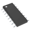
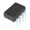
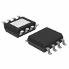
The L6599D is a dual-channel adjustable synchronous buck switching power supply controller that provides 50 percent complementary duty cycle. The high-side switch and low-side switch drivers operate in sync at the correct time and are 180 degrees out of phase. The adjustment of the output voltage is achieved by adjusting the operating frequency. To ensure soft switching, a fixed dead time is inserted between closing one switch and opening the other, thus supporting high-frequency operation. L6599D is available in dual row 16-pin SO and DIP packages. Its operating voltage range is 8.85 to 16V, its operating temperature range is -40°C to 150°C, and its power consumption is 0.83W.
Alternatives and equivalents:
• ISL6504ACBN
• ISL6504CBN-T
• L6599DTR
Line sensing function of L6599D
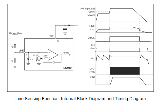
This feature will essentially stop the operation of the IC when the input voltage to the converter falls below a specified range and restart when the voltage returns to within the range. The sensed voltage can be the rectified and filtered supply voltage (in which case this function will act as brownout protection), or in systems with a PFC pre-regulator front end, as the output voltage of the PFC stage (At this time, this function will be used as a power-on and power-off sequence). The L6599D's shutdown at input undervoltage is achieved through an internal comparator, with its non-inverting input at pin 7 (LINE), as shown in the figure. The comparator has an internal reference voltage of 1.25V and if the voltage applied on the LINE pin is lower than this internal reference voltage, the comparator disables the IC. Under these conditions, soft-start discharges, the PFC_STOP pin turns on, and the IC's power consumption is reduced. When the voltage on the pin is higher than the reference voltage, PWM operation is re-enabled.
It is worth noting that the comparator has current hysteresis rather than the more common voltage hysteresis: the internal 1 µA current absorber turns on whenever the voltage on the LINE pin is lower than the reference voltage, and turns off if the voltage is higher than the reference voltage. This approach provides an additional degree of freedom by allowing the user to set the turn-on and turn-off thresholds separately by correctly selecting the resistors of the external voltage divider. In contrast, when using voltage hysteresis, fixing one threshold automatically determines the other, depending on the built-in hysteresis characteristics of the comparator.
Working principle of L6599D
L6599D realizes the regulation and conversion of the input voltage by controlling the switching tube in the resonant circuit. During the working process, the resonant circuit will generate a resonant waveform. Through the control signal inside the L6599D, the resonant waveform can be modulated to control the turn-on and turn-off time of the switch tube. This enables regulation and stabilization of the output voltage.
Application of L6599D
• Telecom SMPS
• LCD and PDP TV
• Desktop PC, entry-level server
• AC-DC adapter, open frame SMPS
Application circuit of L6599D
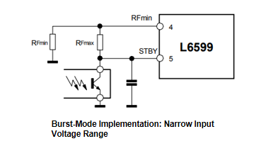
When the resonant half-bridge is lightly loaded or completely unloaded, its switching frequency reaches its maximum value. To ensure that the output voltage is effectively controlled and to prevent soft switching failure, a necessary residual magnetizing current must be maintained in the transformer. However, this current results in a relatively low no-load loss in the converter at no load. The driver can implement pulse intermittent working mode through pin 5 (STBY): if the voltage on pin 5 is lower than 1.25V, the IC will enter an idle state. At this time, both gate drive signals are low level and the oscillator stop working, the soft switching capacitor Css maintains its charging state. In this state, power is consumed only by the 2V voltage reference on the RFmin pin and self-discharge on the Vcc capacitor. When the voltage of pin 5 exceeds 1.25V and is higher than 50mV, the IC will return to normal working status. In order to achieve pulse-intermittent operation, we must relate the voltage at the STBY pin to the feedback loop. The diagram shows the simplest solution, which is suitable for a relatively narrow input voltage range.
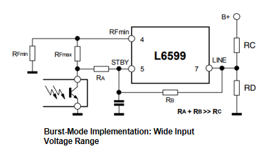
However, the switching frequency of the resonant converter is also affected by the input voltage. If the input voltage range is larger, then the value of PoutB will change significantly for the above diagram. In this case, it is recommended to use the following circuit to introduce the input voltage signal to the STBY pin. Since there is a strong nonlinear relationship between switching frequency and input voltage, experience shows that the change in PoutB can be minimized by adjusting the ratio of RA/(RA+RB). When selecting, make sure the total value of RA+RB is greater than Rc to minimize the impact on the LINE pin voltage.
Common faults and solutions of L6599D
Abnormal working frequency
Abnormal operating frequency of the L6599D power supply controller is usually caused by the following reasons:
Poor pin contact: If the pin contact of L6599D is poor, it may also cause abnormal operating frequency. The solution is to check the soldering condition of the pins and ensure that the pins are well connected to the PCB board.
External component failure: There is a certain correlation between the operating frequency of L6599D and external components. If external components fail, such as inductor damage, capacitor leakage, etc., it may cause abnormal operating frequency. The solution is to check the connections of external components and troubleshoot the problematic components one by one.
Clock signal interference: The operating frequency of L6599D is determined by the clock signal. If the clock signal is interfered with, the operating frequency will be abnormal. The solution is to add a power supply filter circuit to reduce clock signal interference.
The output voltage is unstable
The unstable output voltage of L6599D power controller usually has the following reasons:
Input voltage fluctuation: If the input voltage fluctuation is too large, it will also cause the L6599D output voltage to be unstable. At this time, we need to take appropriate measures, such as adding an input voltage filter circuit, adding a voltage regulator, etc., to ensure the stability of the input voltage.
Large load changes: When the load current changes suddenly, L6599D may not be able to adjust the output voltage in time. The solution is to rationally design the output circuit and add a voltage stabilizing circuit and a filter circuit to ensure the stability of the output voltage.
Inappropriate operating frequency: The operating frequency of L6599D needs to match the operating frequency of the entire power system. If the operating frequency is improperly selected, the output voltage will also be unstable. The solution is to reasonably select a suitable operating frequency and make corresponding parameter adjustments.
Chip overheating
L6599D power controller overheating is usually caused by the following reasons:
Excessive load current: If the load current is too high, the L6599D may not work properly, resulting in overheating of the chip. The solution is to choose a suitable power supply chip according to the load current requirement and ensure that the load current is within the specified range of the chip.
High operating temperature: When L6599D is working in a high temperature environment, its operating temperature may exceed the limit range, resulting in chip overheating. The solution is to reduce the chip temperature by heat dissipation design, such as adding heat sinks, fans, etc..
Excessive power supply current: If the input power supply current is too high, the power consumption of the chip will increase, resulting in higher chip temperature. The solution is to reasonably select the input power supply when designing the power supply system, and ensure that the input power supply current is within the specified range of the chip.
Typical electrical performance of L6599D
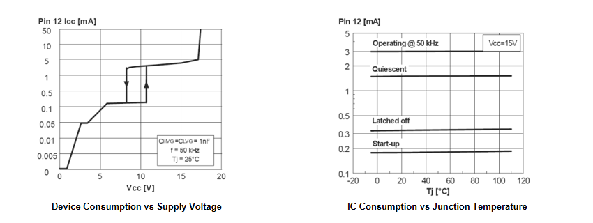
How does the L6599D power controller achieve efficient power conversion and energy transmission?
Optimized design: The circuit design and component selection of the L6599D have been optimized to reduce internal losses and improve overall efficiency. For example, it uses low-loss inductors and capacitors and optimizes the switching frequency.
Soft-switching technology: The resonant flyback technology used in the L6599D is actually a soft-switching technology. Compared with the traditional hard-switching technology, the soft-switching technology can reduce the switching loss during the switching process and improve the system efficiency.
Control strategy: L6599D realizes precise regulation of output voltage and current by precisely controlling the on and off times of the switching tubes. This control strategy enables the power supply system to maintain efficient operation under different load conditions, further improving the energy transfer efficiency.
Resonant Flyback technology: The L6599D utilizes the resonant characteristics of inductance and capacitance between the switching tube's full conduction and shutdown to improve system efficiency and stability. It does this by processing the input current and converting it into two sinusoidal waveform signals, located on the high voltage side and the low voltage side. The mutual coupling of these two signals realizes zero voltage switching (ZVS) and zero current switching (ZCS). This switching method effectively reduces the switching losses and thus improves the energy conversion efficiency.
Frequently Asked Questions [FAQ]
1. What is a switching controller?
A switching regulator can convert input direct current (DC) voltage to the desired direct current (DC) voltage. In an electronic or other device, a switching regulator takes the role of converting the voltage from a battery or other power source to the voltages required by subsequent systems.
2. What are the typical applications of L6599D?
L6599D is commonly used in high-power applications such as power supplies for plasma display panels, telecom, and industrial SMPS (Switched Mode Power Supplies).
3. What are the key features of L6599D?
The key features of L6599D include high-voltage start-up current source, wide-range oscillator frequency (30 kHz - 500 kHz), adjustable dead-time, soft-start time, input/output synchronisation for multi-rails applications, and a built-in driver for the primary MOSFET.
About us
ALLELCO LIMITED
Read more
Quick inquiry
Please send an inquiry, we will respond immediately.
BTS5030-1EJA Power Switch Comprehensive Overview and Applications
on August 30th
Understanding the ADUM1201BRZ-RL7: Specifications, Performance and PCB Layout Tips
on August 30th
Popular Posts
-
What is GND in the circuit?
on January 1th 3036
-

RJ-45 Connector Guide: RJ-45 Connector Color Codes, Wiring Schemes, R-J45 Applications, RJ-45 Datasheets
on January 1th 2607
-

Fiber Connector Types: SC Vs LC And LC Vs MTP
on January 1th 2162
-
Understanding Power Supply Voltages in Electronics VCC, VDD, VEE, VSS, and GND
on November 13th 2067
-

Comparison Between DB9 and RS232
on January 1th 1789
-

What Is An LR44 Battery?
Electricity, that ubiquitous force, quietly permeates every aspect of our daily lives, from trivial gadgets to life-threatening medical equipment, it plays a silent role. However, truly grasping this energy, especially how to store and efficiently output it, is no easy task. It is against this background that this article will focus on a type of coin cell battery that may seem insignificant on the...on January 1th 1754
-
Understanding the Fundamentals:Inductance Resistance, andCapacitance
In the intricate dance of electrical engineering, a trio of fundamental elements takes center stage: inductance, resistance, and capacitance. Each bears unique traits that dictate the dynamic rhythms of electronic circuits. Here, we embark on a journey to decipher the complexities of these components, to uncover their distinct roles and practical uses within the vast electrical orchestra. Inductan...on January 1th 1704
-

CR2430 Battery Comprehensive Guide: Specifications, Applications and Comparison to CR2032 Batteries
What is CR2430 battery ?Benefits of CR2430 BatteriesNormCR2430 Battery ApplicationsCR2430 EquivalentCR2430 VS CR2032Battery CR2430 SizeWhat to look for when buying the CR2430 and equivalentsData Sheet PDFFrequently Asked Questions Batteries are the heart of small electronic devices. Among the many types available, coin cells play a crucial role, commonly found in calculators, remote controls, and ...on January 1th 1640
-
What Is RF and Why Do We Use It?
Radio Frequency (RF) technology is a key part of modern wireless communication, enabling data transmission over long distances without physical connections. This article delves into the basics of RF, explaining how electromagnetic radiation (EMR) makes RF communication possible. We will explore the principles of EMR, the creation and control of RF signals, and their wide-ranging uses. The article ...on January 1th 1620
-
Comprehensive guide to hFE in transistors
Transistors are crucial components in modern electronic devices, enabling signal amplification and control. This article delves into the knowledge surrounding hFE, including how to select a transistor's hFE value, how to find hFE, and the gain of different types of transistors. Through our exploration of hFE, we gain a deeper understanding of how transistors work and their role in electronic circu...on November 13th 1562

