Application and Performance Analysis of XCF32PFSG48C in FPGA Configuration
Catalog
Overview of XCF32PFSG48C
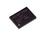
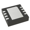
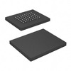
The XCF32PFSG48C, manufactured by Xilinx, is a EEPROM (electrically erasable programmable read-only memory) chip primarily designated for deployment within FPGA (Field-Programmable Gate Array) configurations. Encased in a TFBGA-48 package and employing the SMD or SMT methodology, this electronic component ensures efficient integration within circuitry setups. Operating within a temperature range of -40°C to 85°C is imperative for its optimal functionality. With a requisite supply voltage spanning from 1.65V to 2V, it offers robust operational parameters. Notably, boasting a memory capacity of 32 Mbit, this chip is adept at facilitating diverse computational tasks within electronic systems.
TXB0104PWR is widely used in a variety of medical equipment, automotive electronics, digital circuits, industrial automation, communication equipment and other fields. automation, communication equipment, etc. For example, it can also be used for level conversion of communication protocols such as I2C, SPI, UART, etc. to realize interconnection between different devices. In addition, it can be used to connect low-level microcontrollers (MCUs) to high-level peripheral devices (e.g., LCDs, LEDs, sensors, etc.) for data transmission and control.
Alternative models:
Symbol, footprint and 3D model of XCF32PFSG48C

Manufacturer of XCF32PFSG48C
The XCF32PFSG48C is manufactured by Xilinx. The company was founded in 1984 and is headquartered in San Jose, California. With 3,500 patents and 60 industry firsts, Xilinx has achieved many historic achievements. As the inventor of FPGA, programmable SoC and ACAP, Xilinx was inducted into the U.S. Inventors Hall of Fame in 2009 for its invention of field programmable gate array (FPGA). A few years ago, Xilinx launched a strategic transformation from an FPGA company to an All Programmable company. With the advantage of being fully programmable, Xilinx is entering a broad market beyond traditional FPGAs and plans to achieve substantial growth in revenue within a few years. The company serves a broad range of industrial IoT applications such as robotics, medical, video surveillance, smart grids, transportation, smart factories, and more.
Reset and power-on reset activation
At power up, the device requires the VCCINT power supply to monotonically rise to the nominal operating voltage within the specified VCCINT rise time. If the power supply cannot meet this requirement, then the device might not perform power-on reset properly. During the power -up sequence, OE/RESET' is held Low by the PROM. Once the required supplies have reached their respective POR (Power On Reset) thresholds, the OE/RESET' release is delayed (TOER minimum) to allow more margin for the power supplies to stabilize before initiating configuration. The OE/RESET pin is connected to an external 4.7 kΩ pull-up resistor and also to the target FPGA's INIT pin. For systems utilizing slow-rising power supplies, an additional power monitoring circuit can be used to delay the target configuration until the system power reaches minimum operating voltages by holding the OE/RESET' pin Low. When OE/RESET' is released, the FPGA's INIT pin is pulled High allowing the FPGA's configuration sequence to begin. If the power drops below the power-down threshold (VCCPD), the PROM resets and OE/RESET' is again held Low until the after the POR threshold is reached. OE/RESET' polarity is not programmable. These power-up requirements are shown graphically in the figure. For a fully powered Platform Flash PROM, a reset occurs whenever OE/RESET' is asserted (Low) or CE' is deasserted (High). The address counter is reset, CEO' is driven High, and the remaining outputs are placed in a high-impedance state.

Note:
The XCF32PFSG48C PROM only requires VCCINT to rise above its POR threshold before releasing OE/RESET.
The XCF32PFSG48C PROM requires both VCCINT to rise above its POR threshold and for VCCO to reach the recommended operating voltage level before releasing OE/RESET.
Specifications of XCF32PFSG48C
• Its operating supply current is 10 mA.
• Its power supply voltage is 1.65 V to 2 V.
• Its maximum operating frequency is 50 MHz.
• Its memory capacity is 32 Mbit.
• The brands of XCF32PFSG48C are AMD/Xilinx.
• XCF32PFSG48C operates at -40°C to 85°C.
• Its installation method is SMD or SMT.
• The XCF32PFSG48C features 48 pins and comes in a TFBGA-48 package, housed in a tray.
• The length of the XCF32PFSG48C is 9 mm, the width is 8 mm, and the height is 0.86 mm.
Programming of XCF32PFSG48C
The Platform Flash PROM is a reprogrammable NOR flash device. Reprogramming requires an erase followed by a program operation. A verify operation is recommended after the program operation to validate the correct transfer of data from the programmer source to the Platform Flash PROM. Several programming solutions are available.
External programming
In traditional manufacturing environments, third-party device programmers can program Platform Flash PROMs with an initial memory image before the PROMs are assembled onto boards. Contact a preferred third-party programmer vendor for Platform Flash PROM support information. A sample list of third-party programmer vendors with Platform Flash PROM support is available on the Xilinx web page for Third-Party Programmer Device Support. Pre-programmed PROMs can be assembled onto boards using the typical soldering process guidelines in UG112, Device Package User Guide. A pre-programmed PROM’s memory image can be updated after board assembly using an in-system programming solution.
In-system programming
In-System Programmable PROMs can be programmed individually, or two or more can be daisy-chained together and programmed in-system via the standard 4-pin JTAG protocol as shown in the following figure.
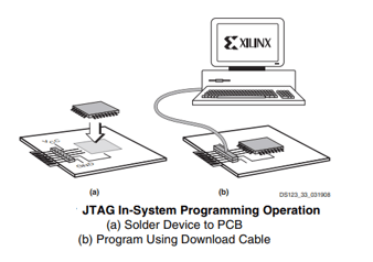
In-system programming offers quick and efficient design iterations and eliminates unnecessary package handling or socketing of devices. The programming data sequence is delivered to the device using either Xilinx iMPACT software and a Xilinx download cable, a third-party JTAG development system, a JTAG -compatible board tester, or a simple microprocessor interface that emulates the JTAG instruction sequence. The iMPACT software also outputs serial vector format (SVF) files for use with any tools that accept SVF format, including automatic test equipment. During in-system programming, the CEO' output is driven High. All other outputs are held in a high-impedance state or held at clamp levels during in-system programming. All non-JTAG input pins are ignored during in-system programming, including CLK, CE, CF, OE/RESET, BUSY, EN_EXT_SEL, and REV_SEL[1:0]. In-system programming is fully supported across the recommended operating voltage and temperature ranges. Embedded, in-system programming reference designs, such as XAPP058, Xilinx In-System Programming Using an Embedded Microcontroller, are available on the Xilinx web page for PROM Programming and Data Storage Application Notes.
In which emerging fields does XCF32PFSG48C have potential value?
XCF32PFSG48C is mainly applied to the configuration of Xilinx FPGAs in the following fields:
Intelligent networked vehicles: With the development of autonomous driving technology, FPGAs are more and more widely used in intelligent networked vehicles. In terms of vehicle perception, XCF32PFSG48C can process raw data from various sensors (e.g. camera, radar, LIDAR, etc.) in real time to extract key information such as road information, vehicle position, obstacle detection, etc., and provide accurate environment perception capability for the automatic driving of vehicles.
Quantum computing: FPGAs are used to build control and scheduling systems for quantum computers, realizing high-speed data transmission and real-time feedback between quantum bits. In the field of quantum computing, XCF32PFSG48C can realize flexible configuration of quantum computing control units through its programmability. This means that researchers can customize the design and optimization of the control unit according to specific quantum computing tasks and hardware platforms. Meanwhile, the high-speed read or write performance of XCF32PFSG48C also ensures the real-time and accuracy of data transmission between quantum bits.
Edge computing: In the field of edge computing, devices need to have fast response and data processing capabilities. with its high-speed data transmission capability and FPGA configuration function, XCF32PFSG48C helps to enhance the performance and flexibility of edge devices to meet the needs of real-time processing and data storage.
Quantitative finance: FPGAs are widely used to accelerate the computation of complex financial models in areas such as high-frequency trading and risk management, etc. The XCF32PFSG48C is particularly suitable for building customized financial trading systems. With its excellent performance and flexible configuration capability, it can provide powerful support for financial trading systems. By using the XCF32PFSG48C, financial trading systems can achieve higher transaction speeds and responsive performance, thus gaining an edge in the competitive marketplace.
Artificial intelligence and machine learning accelerators: FPGAs play an important role in accelerating the deep learning inference and training process. The XCF32PFSG48C can be used to build customized deep learning gas pedals to improve the performance and efficiency of models. First, with the parallel processing capability of FPGAs, we can optimize the computational process of deep learning models to improve computational efficiency and reduce inference and training time. Second, it can store and configure the parameters and instructions of the deep learning model to ensure that the model can run correctly and efficiently. In addition, the high-speed data transfer capability of the XCF32PFSG48C enables the deep learning gas pedal to process a large amount of input data in real time and quickly output inference results, thus meeting the real-time requirements of practical applications.
5G communication: FPGAs play a key role in 5G base stations and terminal equipment for processing high-speed data streams and implementing complex signal processing algorithms. With development tools such as Xilinx Vivado, developers can custom program the XCF32PFSG48C according to specific application requirements to implement efficient communication protocol stacks, baseband processing algorithms, and RF signal transceiver and control functions. In addition, XCF32PFSG48C can also work with other types of processors (such as CPU or DSP) to accomplish complex communication tasks.
Frequently Asked Questions [FAQ]
1. What type of flash memory is XCF32PFSG48C?
XCF32PFSG48C is a NOR flash memory, which is commonly used in embedded systems and for firmware storage.
2. What is the replacement and equivalent of XCF32PFSG48C?
You can replace the XCF32PFSG48C with XCF32PFS48C, XCF32PVOG48C, XCF16PVO48C, XCF16PVOG48C or XCF08PFSG48C.
3. What are some typical applications of XCF32PFSG48C?
XCF32PFSG48C is often used in various embedded systems, including automotive electronics, industrial controls, networking equipment, and consumer electronics, for storing firmware, configuration data, or boot code.
About us
ALLELCO LIMITED
Read more
Quick inquiry
Please send an inquiry, we will respond immediately.
LM358P Guideline Guide: Generation, Application, and Design
on September 2th
TPS54202DDCR High Efficiency Buck Converter Technical Characteristics and Application Guide
on September 2th
Popular Posts
-

What is GND in the circuit?
on January 1th 3329
-

RJ-45 Connector Guide: RJ-45 Connector Color Codes, Wiring Schemes, R-J45 Applications, RJ-45 Datasheets
on January 1th 2856
-
Understanding Power Supply Voltages in Electronics VCC, VDD, VEE, VSS, and GND
on November 21th 2803
-

Fiber Connector Types: SC Vs LC And LC Vs MTP
on January 1th 2287
-

Comparison Between DB9 and RS232
on January 1th 1905
-

What Is An LR44 Battery?
Electricity, that ubiquitous force, quietly permeates every aspect of our daily lives, from trivial gadgets to life-threatening medical equipment, it plays a silent role. However, truly grasping this energy, especially how to store and efficiently output it, is no easy task. It is against this background that this article will focus on a type of coin cell battery that may seem insignificant on the...on January 1th 1865
-

What Is RF and Why Do We Use It?
Radio Frequency (RF) technology is a key part of modern wireless communication, enabling data transmission over long distances without physical connections. This article delves into the basics of RF, explaining how electromagnetic radiation (EMR) makes RF communication possible. We will explore the principles of EMR, the creation and control of RF signals, and their wide-ranging uses. The article ...on January 1th 1848
-

Understanding the Fundamentals:Inductance Resistance, andCapacitance
In the intricate dance of electrical engineering, a trio of fundamental elements takes center stage: inductance, resistance, and capacitance. Each bears unique traits that dictate the dynamic rhythms of electronic circuits. Here, we embark on a journey to decipher the complexities of these components, to uncover their distinct roles and practical uses within the vast electrical orchestra. Inductan...on January 1th 1837
-
Comprehensive guide to hFE in transistors
Transistors are crucial components in modern electronic devices, enabling signal amplification and control. This article delves into the knowledge surrounding hFE, including how to select a transistor's hFE value, how to find hFE, and the gain of different types of transistors. Through our exploration of hFE, we gain a deeper understanding of how transistors work and their role in electronic circu...on November 21th 1831
-

CR2430 Battery Comprehensive Guide: Specifications, Applications and Comparison to CR2032 Batteries
What is CR2430 battery ?Benefits of CR2430 BatteriesNormCR2430 Battery ApplicationsCR2430 EquivalentCR2430 VS CR2032Battery CR2430 SizeWhat to look for when buying the CR2430 and equivalentsData Sheet PDFFrequently Asked Questions Batteries are the heart of small electronic devices. Among the many types available, coin cells play a crucial role, commonly found in calculators, remote controls, and ...on January 1th 1828
