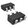
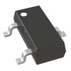
Understanding the TPS7A11 Low-Dropout Voltage Regulator
This article delves into the TPS7A11, a low dropout voltage regulator known for its low quiescent current and ability to operate close to the input voltage. The piece explores the IC's specifications, performance features, and various applications, emphasizing its utility in modern electronic devices. Through comparative analysis with alternatives like the TPS7A26, and detailed discussion on circuit configurations and pin roles, the article offers a comprehensive look at the TPS7A11's capabilities and advantages in both technical and practical terms.Catalog
Overview of the TPS7A11 IC
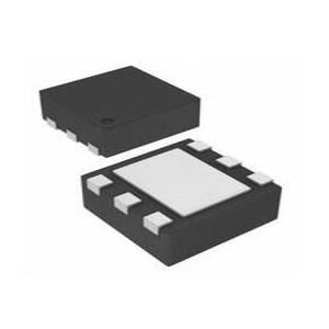
The TPS7A11 is a sophisticated low dropout voltage regulator, recognized for its compact size and remarkably low quiescent current. Designed with subtlety, it can connect to power sources just 140 mV above the desired output. This is achieved through the intricate VBIAS feature, allowing it to function effectively with very low input voltages. This design nuance makes the TPS7A11 exceptionally suited for battery-operated devices, where both efficiency and space are often delicate balances to strike.
TPS7A11 IC Alternative
• TPS7A26
TPS7A11 IC Features
Transient Response and Impedance
The TPS7A11 excels in transient response due to its unique design featuring a combination of high input impedance and low output impedance. Such a configuration allows it to swiftly adapt to fluctuations in input supply, while minimizing noise. This characteristic proves invaluable in many applications, ensuring stable performance even in unpredictable power environments and contributing to a sense of reliability.
Undervoltage Lockout Mechanism
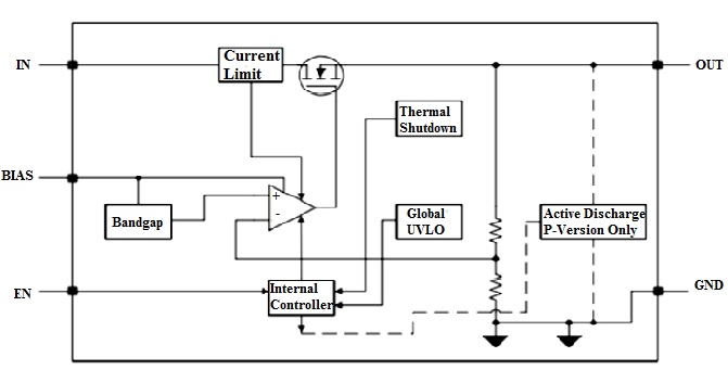
A global undervoltage lockout mechanism is integrated, strategically delaying LDO activation until BIAS and IN voltages exceed their lockout thresholds. This dual-circuit approach mitigates risks of untimely activation, comforting those who seek to protect sensitive electronics from harm.
Active Discharge and Voltage Regulation
Active discharge employs a pulldown MOSFET, providing meticulous voltage control for a variety of practical applications. This capability for rapid voltage regulation enhances the device's versatility, meeting diverse operational necessities with precision.
Protective Mechanisms
The TPS7A11 incorporates internal foldback current limits, offering formidable protection from overcurrent events. Moreover, the thermal shutdown circuit acts as a guardian, disabling the LDO temporarily until temperatures return to safer levels. This adaptive process helps avert damage, mirroring its commitment to sustained operational health.
Operational Modes
Skillfully transitioning through normal, dropout, and disabled modes, the device adjusts output performance as needed. This adaptability highlights its proficiency in maintaining function amid changing conditions, demonstrating a keen awareness of environmental influences.
The TPS7A11 represents an elegant fusion of features: swift response, protective strategies, and flexible operations, making it a fitting choice for contemporary electronic applications.
TPS7A11 Circuit Configuration
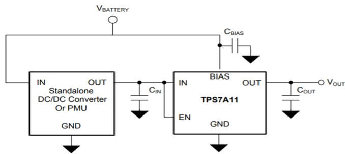
Designing circuits with the TPS7A11 invites careful selection of external components, which shapes performance and stability. Components like capacitors play important roles here.
Ceramic capacitors are favored for their consistent stability and reliability. For input and output needs, 2.2 µF typically addresses filtering and noise reduction, maintaining power supply integrity in varied load conditions. Matching capacitors to specific voltage ratings to guard against early failures.
Typically set at 0.1 µF, the bias capacitor uplifts regulator stability and transient response. It supports voltage stability for the bias rail, ensuring seamless TPS7A11 operation. Fine-tuning these specs can reveal reliability gains, stressing the worth of detailed testing in development.
In component positioning, strategic proximity to the TPS7A11 limits parasitic inductance and resistance, for high-frequency tasks. Considerations like temperature and humidity subtly influence component behavior. Ceramic capacitors may react to temperature shifts, prompting the choice of suitable temperature coefficients.
TPS7A11 Pin Configuration
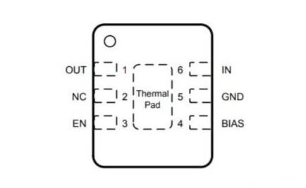
Output (OUT)
The output pin is needed in providing stable voltage. It's crafted to uphold precise voltage levels despite fluctuating loads. Connections should aim to minimize resistance, helping to prevent power losses and ensuring reliability in varied environments.
Enable (EN)
The enable pin dictates the regulator's operating mode, for power management in battery-dependent devices. It facilitates toggling between active and low-energy states, and practical use in mobile tech showcases notable improvements in battery longevity.
Bias (BIAS)
This pin provides voltage for internal circuits, influencing low dropout voltage and efficiency. Thoughtful design of the bias network, supported by comprehensive empirical analysis, fosters stability and boosts regulator efficiency.
Input (IN)
Responsible for supply voltage reception, the input pin needs connection to a stable power source. Employing sound filtering techniques is good to block noise interference. Industry-aligned design principles help mitigate disruptions, ensuring steady input conditions.
TPS7A11 Package Variations
DRV Package
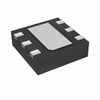
This 6-pin package merges functionality with compactness. Its design eases efficient heat dissipation, for high-performance applications like automotive systems. Effective thermal dynamics contribute to DRV package functionality. Proper connections of thermal pads to the ground enhance heat dissipation and lower impedance, which can subtly boost device performance. The thermal simulation software, a tool that assists in refining pad placement, leading to optimal heat management and the graceful aging of devices.
DSBGA (YKA) Package
Offering an ultraminiature solution, the 5-pin DSBGA package is ideal for portable and wearable tech. It supports minimal footprint designs while maintaining power management prowess, proven effective in consumer electronics with densely packed circuit layouts. Celebrated for its compactness and functionality, the DSBGA package facilitates high-density circuit boards. This package design is a favored choice for mobile and portable devices because of its ability to integrate multiple features in constrained spaces. Such an approach not only optimizes performance but also modestly shrinks the device's physical footprint.
TPS7A11 Specifications
|
Specifications |
Details |
|
Voltage Range (Output) |
0.75V to 3.3V |
|
Package Options |
DRV, YKA |
|
Ultra-Low Dropout (DRV Package) |
140mV 500mA |
|
Ultra-Low Dropout (YKA Package) |
110mV |
|
Quiescent Current (VIN) |
1.6 µA |
|
Quiescent Current (VBIAS) |
6 µA |
|
Accuracy (Load, Line, Temperature) |
1.50% |
|
Power Supply Rejection Ratio (PSRR) |
64dB at 1 kHz |
|
Active Output Discharge |
Yes |
|
Fixed Output Voltage Options |
0.5V to 3V |
|
VBIAS Range |
1.7V to 5.5V |
|
Operating Junction Temperature Range |
-40°C to 125°C |
|
Output Voltage Range at Operating Temp |
0.5V to 3V |
|
Bias Capacitor Requirement |
0.1 µF |
|
Maximum ESR at Operating Temp |
< 250mΩ |
TPS7A11 Applications
Supplying Power
The TPS7A11 plays a role in delivering power to the lower core voltages of contemporary microcontrollers and sensors. This provides a stable foundation for their intricate operations, allowing them to perform with precision.
Wearable Technology
This voltage regulator finds its way into smartwatches and fitness trackers, silently supporting their functionality as they track your movements and health metrics.
Audio
Wireless headphones and earbuds benefit from the TPS7A11, ensuring consistent performance that resonates with quality during your daily listening experiences.
Imaging Devices
Incorporated into camera modules, the TPS7A11 contributes to capturing moments with clarity, supporting the complex circuits needed for high-quality imaging.
Portable and Smart Devices
The TPS7A11 is also embraced within portable medical devices, smartphones, tablets, and solid-state devices. Its presence is felt in the seamless operation of these technologies, meeting the ever-evolving needs of modern life.
Conclusion
The TPS7A11 IC stands out as a versatile and efficient voltage regulator for modern electronic applications. Through its detailed examination of performance features, package options, and practical applications, this article shows the importance of advanced IC design in enhancing device functionality and energy efficiency. The insights provided not only illuminate the technical specifications of the TPS7A11 but also reflect on its broader impact in the field of electronics, showcasing the intersection of innovation and practical application in shaping the future of technology.
About us
ALLELCO LIMITED
Read more
Quick inquiry
Please send an inquiry, we will respond immediately.

All You Need to Know About the FHP100N07 MOSFET
on October 2th
IRF540N Transistor Overview Applications and Features
on October 2th
Popular Posts
-
What is GND in the circuit?
on January 1th 2933
-

RJ-45 Connector Guide: RJ-45 Connector Color Codes, Wiring Schemes, R-J45 Applications, RJ-45 Datasheets
on January 1th 2488
-

Fiber Connector Types: SC Vs LC And LC Vs MTP
on January 1th 2080
-
Understanding Power Supply Voltages in Electronics VCC, VDD, VEE, VSS, and GND
on November 8th 1874
-

Comparison Between DB9 and RS232
on January 1th 1759
-

What Is An LR44 Battery?
Electricity, that ubiquitous force, quietly permeates every aspect of our daily lives, from trivial gadgets to life-threatening medical equipment, it plays a silent role. However, truly grasping this energy, especially how to store and efficiently output it, is no easy task. It is against this background that this article will focus on a type of coin cell battery that may seem insignificant on the...on January 1th 1709
-
Understanding the Fundamentals:Inductance Resistance, andCapacitance
In the intricate dance of electrical engineering, a trio of fundamental elements takes center stage: inductance, resistance, and capacitance. Each bears unique traits that dictate the dynamic rhythms of electronic circuits. Here, we embark on a journey to decipher the complexities of these components, to uncover their distinct roles and practical uses within the vast electrical orchestra. Inductan...on January 1th 1649
-
CR2430 Battery Comprehensive Guide: Specifications, Applications and Comparison to CR2032 Batteries
What is CR2430 battery ?Benefits of CR2430 BatteriesNormCR2430 Battery ApplicationsCR2430 EquivalentCR2430 VS CR2032Battery CR2430 SizeWhat to look for when buying the CR2430 and equivalentsData Sheet PDFFrequently Asked Questions Batteries are the heart of small electronic devices. Among the many types available, coin cells play a crucial role, commonly found in calculators, remote controls, and ...on January 1th 1537
-
What Is RF and Why Do We Use It?
Radio Frequency (RF) technology is a key part of modern wireless communication, enabling data transmission over long distances without physical connections. This article delves into the basics of RF, explaining how electromagnetic radiation (EMR) makes RF communication possible. We will explore the principles of EMR, the creation and control of RF signals, and their wide-ranging uses. The article ...on January 1th 1533
-

CR2450 vs CR2032: Can The Battery Be Used Instead?
Lithium manganese batteries do have some similarities with other lithium batteries. High energy density and long service life are the characteristics they have in common. This kind of battery has won the trust and favor of many consumers because of its unique safety. Expensive tech gadgets? Small appliances in our homes? Look around and you'll see them everywhere. Among these many lithium-manganes...on January 1th 1500
