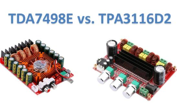
TDA7498E vs. TPA3116D2: Which Amplifier Stands Out?
In the world of digital audio amplification, choosing the right amplifier can significantly elevate sound quality and system efficiency. Two standout models, the TDA7498E and TPA3116D2, cater to diverse audio needs, from enhancing home theater setups to powering professional speakers. This article provides an in-depth analysis of these amplifiers, examining their unique features, maximum ratings, thermal management, and technical specifications. By comparing their strengths and limitations, this guide aims to assist you in making informed decisions and aligning amplifier choices with specific performance requirements and environmental conditions.Catalog
Overview of the TDA7498E
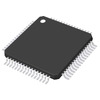
The TDA7498E, a highly advanced Class-D audio amplifier, stands out for its dual bridge-tied load (BTL) configuration and compatibility with a single power source. Such features make it a superb option for home audio systems and active speaker setups. Utilizing a highly efficient 36-pin PowerSSO package, which includes an exposed pad, the design effectively manages heat. This aspect is basic for sustaining performance and extending lifespan over time.
The amplifier incorporates state-of-the-art technology focused on reducing energy loss, a consideration that not only lowers operational expenses but also lessens environmental burdens. The use of a single power source streamlines the structural design, ensuring ease of assembly and bolstering reliability. You can value the amplifier for its harmonious balance between power efficiency and sound quality, reflecting its impressive engineering prowess.
In modern audio installations, space can be a dangerous constraint. The TDA7498E, with its compact yet powerful design, adeptly tackles these spatial limitations. Its efficiency results in cooler operation and decreases the demand for extensive cooling systems. You can understand the importance of maintaining audio consistency across diverse scenarios. This amplifier meets the demand for reliability effectively, providing continuous high-quality sound output regardless of conditions.
Overview of the TPA3116D2
The TPA3116D2 is recognized as a tremendously efficient stereo digital amplifier, which has played a key role in advancing audio technology by powering speakers up to 100W at 2Ω in a mono setup. This amplifier is crafted for greater adaptability, showcasing its versatility by delivering 2 × 15 W output without needing an external heatsink on a single-layer PCB. For scenarios requiring enhanced power, it can effectively supply 2 × 50 W at 4Ω with minimal heatsink demands. This flexibility caters to various audio amplification needs, spanning from consumer electronics to professional audio equipment.
A striking attribute of the TPA3116D2 is its functionality in both master and slave modes. It utilizes an innovative oscillator/PLL system aimed at reducing AM interference, an obstacle that commonly impacts sound quality and diminishes auditory pleasure. This sophisticated system also supports the synchronization of multiple units, a beneficial feature for intricate audio setups where clean timing is essential. You can discover that this synchronization capability markedly boosts audio performance by ensuring even sound distribution across all speakers.
Safety and dependability are threads woven into the fabric of the TPA3116D2. It integrates comprehensive fault protection features such as short-circuit, thermal, and voltage protections. These precautions contribute to a long lifespan and steadfast reliability, rendering the amplifier resistant to potential overloads. You can value these protections as they offer reassurance, knowing components are safeguarded from common electrical hazards that might occur during operation.
Maximum Ratings for TDA7498E and TPA3116D2
TDA7498E Absolute Maximum Ratings
|
Symbol |
Parameter |
Value |
Unit |
|
VCC |
DC supply voltage for pins PVCCA, PVCCB, SVCC |
45 |
V |
|
VI |
Voltage limits for input pins STBY, MUTE, INNA, INPA,
INNB, INPB, GAIN, MODE |
-0.3 to 4.0 |
V |
|
Tj |
Operating junction temperature |
0 to 150 |
°C |
|
Top |
Operating ambient temperature |
0 to 70 |
°C |
|
Tstg |
Storage temperature |
-40 to 150 |
°C |
TPA3116D2 Absolute Maximum Ratings
|
Parameter |
Pins/Signals |
Min |
Max |
Unit |
|
Supply voltage, VCC |
PVCC, AVCC |
–0.3 |
30 |
V |
|
Input voltage, VI |
INPL, INNL, INPR, INNR |
–0.3 |
6.3 |
V |
|
PLIMIT, GAIN / SLV, SYNC |
–0.3 |
GVDD+0.3 |
V |
|
|
AM0, AM1, AM2, MUTE, SDZ, MODSEL |
–0.3 |
PVCC+0.3 |
V |
|
|
Slew rate, maximum(2) |
AM0, AM1, AM2, MUTE, SDZ, MODSEL |
10 |
V/ms |
|
|
Operating free-air temperature, TA |
–40 |
85 |
°C |
|
|
Operating junction temperature, TJ |
–40 |
150 |
°C |
|
|
Storage temperature, Tstg |
–40 |
125 |
°C |
Thermal Efficiency in the TDA7498E and TPA3116D2
TDA7498E Thermal Information
|
Symbol |
Parameter |
Condition |
Min |
Typ |
Max |
Unit |
|
Iq |
Total quiescent current |
No LC filter, no load |
- |
60 |
- |
mA |
|
IqSTBY |
Quiescent current in standby |
- |
- |
1 |
- |
µA |
|
VOS |
Output offset voltage |
Vi = 0, Av = 23.6 dB, no load |
-20 |
- |
20 |
mV |
|
IOCP |
Overcurrent protection threshold |
RL = 0 Ω |
10 |
11 |
14 |
A |
|
Tj |
Junction temperature at thermal shutdown |
- |
140 |
150 |
160 |
°C |
|
Ri |
Input resistance |
Differential input |
69 |
- |
- |
kΩ |
|
VUVP |
Undervoltage protection threshold |
- |
- |
- |
8 |
V |
|
RdsON |
Power transistor on-resistance |
High side |
- |
0.15 |
- |
Ω |
|
Low side |
- |
0.15 |
- |
Ω |
||
|
Po |
Output power |
THD = 10% |
- |
160 |
- |
W |
|
THD = 1% |
- |
125 |
- |
W |
||
|
Po |
Parallel BTL (mono) output power |
RL = 3 Ω, Vcc = 36 V, THD = 10% |
- |
220 |
- |
W |
|
THD = 1% |
- |
170 |
- |
W |
||
|
η |
Efficiency |
- |
- |
85 |
- |
% |
|
THD |
Total harmonic distortion |
Po = 1 W |
- |
0.05 |
- |
% |
|
GV |
Closed-loop gain |
GAIN < 0.25*VDD |
- |
23.8 |
- |
dB |
|
0.25VDD < GAIN < 0.5VDD |
- |
29.8 |
- |
dB |
||
|
0.5VDD < GAIN < 0.75VDD |
- |
33.3 |
- |
dB |
||
|
GAIN > 0.75*VDD |
- |
35.8 |
- |
dB |
||
|
ΔGV |
Gain matching |
- |
-1 |
- |
1 |
dB |
|
CT |
Crosstalk |
f = 1 kHz, Po = 1 W |
50 |
60 |
- |
dB |
|
Vn |
Total output noise |
Inputs shorted and to ground, A Curve |
- |
231 |
- |
µV |
|
Inputs shorted and to ground, f = 20 Hz to 20 kHz |
- |
400 |
- |
µV |
||
|
SVRR |
Supply voltage rejection ratio |
fr = 100 Hz, Vr = 0.5 Vpp, CSVR = 10 µF |
- |
55 |
- |
dB |
|
Tr, Tf |
Rise and fall times |
- |
- |
35 |
- |
ns |
|
fSW |
Switching frequency |
Internal oscillator |
240 |
310 |
400 |
kHz |
|
fSWR |
Output switching frequency range |
With internal oscillator by changing ROS (1) |
240 |
- |
- |
kHz |
|
VinH |
Digital input high (H) |
- |
2 |
- |
- |
V |
|
VinL |
Digital input low (L) |
- |
- |
0.8 |
- |
V |
|
Function Mode |
Standby, mute, play modes |
STBY < 0.5 V; MUTE = X |
Standby |
|||
|
STBY > 2.5 V; MUTE < L |
Mute |
|||||
|
STBY > 2.5 V; MUTE > H |
Play |
|||||
|
AMUTE |
Mute attenuation |
VMUTE < L, VSTBY = H |
- |
75 |
- |
dB |
TPA3116D2 Thermal Information
|
PARAMETER |
TEST CONDITIONS |
MIN |
TYP |
MAX |
UNIT |
|
VOS |
Class-D output offset voltage (measured differentially),
VI = 0 V, Gain = 36 dB |
1.5 |
15 |
mV |
|
|
ICC |
Quiescent supply current, SDZ = 2 V, No load or filter,
PVCC = 12 V |
20 |
35 |
mA |
|
|
SDZ = 2 V, No load or filter, PVCC = 24 V |
32 |
50 |
mA |
||
|
ICC(SD) |
Quiescent supply current in shutdown mode, SDZ = 0.8 V,
No load or filter, PVCC = 12 V |
<50 |
µA |
||
|
SDZ = 0.8 V, No load or filter, PVCC = 24 V |
50 |
400 |
µA |
||
|
rDS(on) |
Drain-source on-state resistance, measured pin to pin,
PVCC = 21 V, Iout = 500 mA, TJ = 25°C |
120 |
mΩ |
||
|
G |
Gain (BTL), R1 = 5.6 kΩ, R2 = Open |
19 |
20 |
21 |
dB |
|
R1 = 20 kΩ, R2 = 100 kΩ |
25 |
26 |
27 |
dB |
|
|
R1 = 39 kΩ, R2 = 100 kΩ |
31 |
32 |
33 |
dB |
|
|
R1 = 47 kΩ, R2 = 75 kΩ |
35 |
36 |
37 |
dB |
|
|
G |
Gain (SLV), R1 = 51 kΩ, R2 = 51 kΩ |
19 |
20 |
21 |
dB |
|
R1 = 75 kΩ, R2 = 47 kΩ |
25 |
26 |
27 |
dB |
|
|
R1 = 100 kΩ, R2 = 39 kΩ |
31 |
32 |
33 |
dB |
|
|
R1 = 100 kΩ, R2 = 16 kΩ |
35 |
36 |
37 |
dB |
|
|
ton |
Turn-on time, SDZ = 2 V |
10 |
ms |
||
|
tOFF |
Turn-off time, SDZ = 0.8 V |
2 |
µs |
||
|
GVDD |
Gate drive supply, IGVDD < 200 µA |
6.4 |
6.9 |
7.4 |
V |
|
VO |
Output voltage maximum under PLIMIT control, V(PLIMIT) =
2 V; VI = 1 Vrms |
6.75 |
7.9 |
8.75 |
V |
Comparing the Features of TDA7498E and TPA3116D2
Features of the 1N4001
|
Feature |
Details |
|
Output Power |
160 W + 160 W at THD = 10%, RL = 4 Ω, VCC = 36 V |
|
Mono Parallel BTL Output Power |
1 x 220 W at THD = 10%, RL = 3 Ω, VCC = 36 V |
|
Supply Voltage Range |
Wide-range single-supply operation (14 - 36 V) |
|
Efficiency |
High efficiency (η = 85%) |
|
Parallel BTL Function |
Enabled via the MODE pin |
|
Selectable Gain Settings |
Four fixed gain settings: 23.8 dB, 29.8 dB, 33.3 dB, 35.8
dB |
|
Noise Minimization |
Differential inputs minimize common-mode noise |
|
Standby and Mute |
Standby and mute features available |
|
Protection |
Smart protection, thermal overload protection |
|
Offset Voltage |
Small offset less than 20 mV |
Features of the STM32 F4
|
Feature |
Description |
|
Supports Multiple Output Configurations |
- 2 × 50 W into a 4-Ω BTL load at 21 V (TPA3116D2) |
|
- 2 × 30 W into an 8-Ω BTL load at 24 V (TPA3118D2) |
|
|
- 2 × 15 W into an 8-Ω BTL load at 15 V (TPA3130D2) |
|
|
Wide Voltage Range |
4.5 V to 26 V |
|
Efficient Class-D Operation |
- >90% power efficiency |
|
- Low idle loss reduces heat sink size |
|
|
- Advanced modulation schemes |
|
|
Multiple Switching Frequencies |
- AM avoidance |
|
- Master and slave synchronization |
|
|
- Up to 1.2 MHz switching frequency |
|
|
Feedback Power-Stage Architecture |
High PSRR reduces PSU requirements |
|
Programmable Power Limit |
Yes |
|
Input Options |
Differential and single-ended inputs |
|
Mode Options |
Stereo and mono mode with single-filter mono
configuration |
|
Single Power Supply |
Reduces component count |
|
Integrated Self-Protection Circuits |
- Overvoltage |
|
- Undervoltage |
|
|
- Overtemperature |
|
|
- DC detect |
|
|
- Short circuit with error reporting |
|
|
Thermally Enhanced Packages |
- DAD (32-pin HTSSOP pad up) |
|
- DAP (32-pin HTSSOP pad down) |
|
|
Operating Temperature Range |
–40°C to 85°C |
Technical Specifications
Here is a table with the technical specifications, attributes, parameters, and parts with similar specifications to the STMicroelectronics TDA7498E.
|
Type |
Parameter |
|
Lifecycle Status |
Active (Last Updated: 8 months ago) |
|
Mount |
Surface Mount |
|
Mounting Type |
Surface Mount |
|
Package / Case |
36-PowerFSOP (0.295, 7.50mm Width) |
|
Number of Pins |
36 |
|
Operating Temperature |
0°C ~ 70°C TA |
|
Packaging |
Tube |
|
JESD-609 Code |
e3 |
|
Part Status |
Obsolete |
|
Moisture Sensitivity Level (MSL) |
1 (Unlimited) |
|
Number of Terminations |
36 |
|
ECCN Code |
EAR99 |
|
Type |
Class D |
|
Terminal Finish |
Matte Tin (Sn) - annealed |
|
HTS Code |
8542.33.00.01 |
|
Voltage - Supply |
14V ~ 36V |
|
Terminal Position |
DUAL |
|
Terminal Form |
GULL WING |
|
Peak Reflow Temperature (°C) |
260 |
|
Number of Functions |
1 |
|
Terminal Pitch |
0.5mm |
|
Time@Peak Reflow Temperature-Max (s) |
30 |
|
Base Part Number |
TDA7498 |
|
Pin Count |
36 |
|
Output Type |
1-Channel (Mono) or 2-Channel (Stereo) |
|
Supply Voltage-Min (Vsup) |
14V |
|
Number of Channels |
2 |
|
Output Power |
220W |
|
Input Offset Voltage (Vos) |
20mV |
|
Bandwidth |
20 kHz |
|
Voltage Gain |
35.8dB |
|
Max Output Power |
220W |
|
Max Output Power x Channels @ Load |
220W x 1 @ 3 Ω; 160W x 2 @ 4 Ω |
|
Harmonic Distortion |
10% |
|
Features |
Differential Inputs, Mute, Short-Circuit and Thermal
Protection, Standby |
|
Dimensions |
Length: 10.3mm, Width: 7.5mm, Height: 2.45mm |
|
Radiation Hardening |
No |
|
RoHS Status |
ROHS3 Compliant |
Comparison of TDA7498E and TPA3116D2 in Electrical Properties
TDA7498E Electrical Characteristics
|
Thermal Metric (1) |
TPA3130D2 |
TPA3118D2 |
TPA3116D2 |
Unit |
|
Package |
DAP (2) |
DAP (3) |
DAD (4) |
|
|
Pin Count |
32 Pins |
32 Pins |
32 Pins |
|
|
RθJA Junction-to-ambient thermal resistance |
36 |
22 |
14 |
°C/W |
|
ψJT Junction-to-top characterization parameter |
0.4 |
0.3 |
1.2 |
°C/W |
|
ψJB Junction-to-board characterization parameter |
5.9 |
4.7 |
5.7 |
°C/W |
TPA3116D2 Electrical Characteristics
|
Symbol |
Parameter |
Min |
Typ |
Max |
Unit |
|
Rth j-case |
Thermal resistance, junction to case |
- |
3 |
- |
°C/W |
Datasheet PDF
TDA7498E Datasheets:
About us
ALLELCO LIMITED
Read more
Quick inquiry
Please send an inquiry, we will respond immediately.
TIP2955 Transistor: Pinout, Equivalents, and Datasheet
on November 9th
XL4015 DC Buck Converter: Specifications, Substitute, and Pinout
on November 8th
Popular Posts
-
What is GND in the circuit?
on January 1th 3105
-

RJ-45 Connector Guide: RJ-45 Connector Color Codes, Wiring Schemes, R-J45 Applications, RJ-45 Datasheets
on January 1th 2671
-
Understanding Power Supply Voltages in Electronics VCC, VDD, VEE, VSS, and GND
on November 15th 2209
-

Fiber Connector Types: SC Vs LC And LC Vs MTP
on January 1th 2182
-

Comparison Between DB9 and RS232
on January 1th 1802
-

What Is An LR44 Battery?
Electricity, that ubiquitous force, quietly permeates every aspect of our daily lives, from trivial gadgets to life-threatening medical equipment, it plays a silent role. However, truly grasping this energy, especially how to store and efficiently output it, is no easy task. It is against this background that this article will focus on a type of coin cell battery that may seem insignificant on the...on January 1th 1774
-
Understanding the Fundamentals:Inductance Resistance, andCapacitance
In the intricate dance of electrical engineering, a trio of fundamental elements takes center stage: inductance, resistance, and capacitance. Each bears unique traits that dictate the dynamic rhythms of electronic circuits. Here, we embark on a journey to decipher the complexities of these components, to uncover their distinct roles and practical uses within the vast electrical orchestra. Inductan...on January 1th 1728
-

CR2430 Battery Comprehensive Guide: Specifications, Applications and Comparison to CR2032 Batteries
What is CR2430 battery ?Benefits of CR2430 BatteriesNormCR2430 Battery ApplicationsCR2430 EquivalentCR2430 VS CR2032Battery CR2430 SizeWhat to look for when buying the CR2430 and equivalentsData Sheet PDFFrequently Asked Questions Batteries are the heart of small electronic devices. Among the many types available, coin cells play a crucial role, commonly found in calculators, remote controls, and ...on January 1th 1673
-
What Is RF and Why Do We Use It?
Radio Frequency (RF) technology is a key part of modern wireless communication, enabling data transmission over long distances without physical connections. This article delves into the basics of RF, explaining how electromagnetic radiation (EMR) makes RF communication possible. We will explore the principles of EMR, the creation and control of RF signals, and their wide-ranging uses. The article ...on January 1th 1670
-
Comprehensive guide to hFE in transistors
Transistors are crucial components in modern electronic devices, enabling signal amplification and control. This article delves into the knowledge surrounding hFE, including how to select a transistor's hFE value, how to find hFE, and the gain of different types of transistors. Through our exploration of hFE, we gain a deeper understanding of how transistors work and their role in electronic circu...on November 15th 1631


