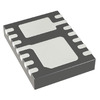
SN74LVC1G17DCKR Single Schmitt-Trigger Buffer: Features, Equivalents, and Datasheet
This article serves as a comprehensive guide, detailing the functionality, applications, and technical intricacies of this innovative device. Through detailed schematic analyses, practical applications, and a review of comparable and substitute components, this article is your gateway to mastering the SN74LVC1G17DCKR's contribution to cutting-edge electronic solutions. This article provide a visual and technical blueprint for implementing the component effectively. Pinout diagrams, rich in detail, illustrate accurate connections, thereby boosting the device's performance across various applications.Catalog
What is the SN74LVC1G17DCKR?
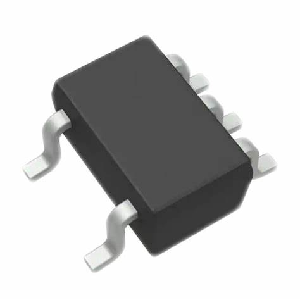
The SN74LVC1G17DCKR is an advanced Schmitt-trigger buffer designed to operate within a voltage range of 1.65V to 5.5V VCC. Encased in an ultra-compact DPW package with a 0.8mm square footprint, it leverages CMOS technology to achieve high output drive while keeping power consumption low. The Schmitt-trigger functionality allows for varying input thresholds, which enhances signal integrity in noisy environments. The Ioff circuitry prevents backflow during partial-power-down conditions, bolstering system reliability.
SN74LVC1G17DCKR Equivalents
• TC7SZ17F
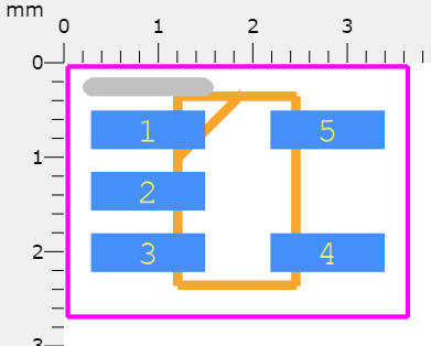
SN74LVC1G17DCKR Pin Configuration
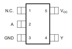
Pin 1 (A - Data Input)
Pin 1, denoted as A, is the data input for the buffer. With the inclusion of Schmitt-Trigger architecture, it assures that input signals suffering from slow rise and fall times are converted into precise digital transitions. This adaptability is beneficial in environments where input noise might otherwise provoke erratic system reactions.
Pin 2 (GND - Ground)
Pin 2 serves as the ground connection. Maintaining proper grounding is important for the device's steady performance, as variations in ground potential might induce unforeseen behavior, especially during high-speed switching operations. Connecting this pin to a stable ground plane helps mitigate electrical interference.
Pin 3 (Y - Data Output)
Pin 3, designated as Y, functions as the data output. This pin, characterized by its low output impedance, provides the necessary drive capability for interfacing with subsequent stages in a circuit. It reflects the input signal state via a Schmitt Trigger, ensuring the delivery of a pristine, noise-free output.
Pin 4 (Vcc - Supply Voltage)
Identified as the supply voltage pin, Pin 4 (Vcc) should be connected to a dependable power source that aligns with the device’s voltage specifications. The SN74LVC1G17DCKR operates within a voltage range of 1.65V to 5.5V. Employing decoupling capacitors close to this pin is advised to filter any supply noise, safeguarding device performance.
Pin 5 (NC - No Connect)
Pin 5 is labeled NC, indicating No Connect. This pin is not connected to the internal circuitry of the IC and can be left unconnected. Alternatively, it might lend structural support depending on the PCB layout.
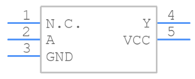
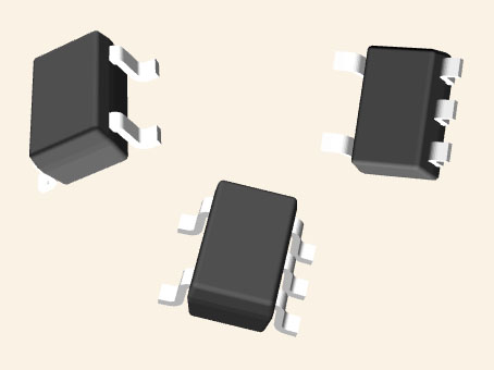
SN74LVC1G17DCKR Symbol, Footprint, and CAD Model
Features of SN74LVC1G17DCKR
Ultra-Small Package Size
The SN74LVC1G17DCKR is presented in an exceptionally compact 0.64mm² package with a 0.5mm pitch. Such minute dimensions are beneficial in contemporary electronics where preserving space is great. This degree of miniaturization empowers you to incorporate the device into space-constrained applications, from portable gadgets to compact industrial equipment.
High Voltage Flexibility
This device functions with up to 5V VCC and can endure input voltages up to 5.5V. Supporting diverse voltage levels makes it ideal for mixed-signal environments. Versatility in voltage adaptation ensures it harmonizes with various electronic components and systems, reducing the risk of voltage mismatches and consequential damage.
Fast Propagation Delay
The SN74LVC1G17DCKR features a maximum propagation delay (tpd) of 4.6ns at 3.3V. This prompt response time is beneficial for applications needing rapid data transmission and minimal latency. For example, in high-speed communication systems, a reduced propagation delay can improve overall system performance by minimizing data bottlenecks.
Low Power Consumption
The device boasts a maximum ICC of 10μA, signifying low power draw. This attribute is valuable for battery-operated and energy-efficient applications, extending operational life and cutting down energy costs.
High Output Drive Capability
Capable of delivering an output drive of ±24mA at 3.3V, the SN74LVC1G17DCKR can handle loads. This functionality is apt for applications that necessitate robust driving power. In practical terms, it guarantees reliable performance when interfacing with various integrated circuits or peripherals.
Ioff Current Management
The device integrates Ioff support for live insertion and back-drive protection. This feature preserves both the device and the system from potential harm caused by unintended current flows during events like hot swapping or power sequence deviations. Such protection is instrumental in modular systems where components are frequently swapped without a complete shutdown.
ESD Protection
The SN74LVC1G17DCKR surpasses multiple ESD protection standards. Enhanced electrostatic discharge protection shields the device from static-induced harm, boosting its reliability and longevity. This is particularly important in environments prone to electrostatic effects, such as manufacturing floors or field operations.
SN74LVC1G17DCKR Specifications
|
Type |
Parameter |
|
Lifecycle Status |
ACTIVE (Last Updated: 3 days ago) |
|
Factory Lead Time |
6 Weeks |
|
Contact Plating |
Gold |
|
Mount |
Surface Mount |
|
Mounting Type |
Surface Mount |
|
Package / Case |
5-TSSOP, SC-70-5, SOT-353 |
|
Number of Pins |
5 |
|
Operating Temperature |
-40°C~125°C TA |
|
Packaging |
Cut Tape (CT) |
|
Series |
74LVC |
|
JESD-609 Code |
e4 |
|
Pbfree Code |
Yes |
|
Part Status |
Active |
|
Moisture Sensitivity Level |
1 (Unlimited) |
|
Number of Terminations |
5 |
|
Termination |
SMD/SMT |
|
ECCN Code |
EAR99 |
|
Packing Method |
TR |
|
Voltage - Supply |
1.65V~5.5V |
|
Terminal Position |
DUAL |
|
Terminal Form |
GULL WING |
|
Peak Reflow Temperature (Cel) |
260 |
|
Number of Functions |
1 |
|
Supply Voltage |
3.3V |
|
Base Part Number |
74LVC1G17 |
|
Pin Count |
5 |
|
Output Type |
Push-Pull |
|
Polarity |
Non-Inverting |
|
Power Supplies |
3.3V |
|
Number of Channels |
1 |
|
Nominal Supply Current |
500nA |
|
Propagation Delay |
11 ns |
|
Quiescent Current |
1.5μA |
|
Input Type |
Schmitt Trigger |
|
Turn On Delay Time |
11 ns |
|
Family |
LVC/LCX/Z |
|
Logic Function |
Buffer, Schmitt Trigger |
|
Number of Inputs |
1 |
|
Logic Type |
Buffer, Non-Inverting |
|
Max I(ol) |
0.024 A |
|
Schmitt Trigger |
YES |
|
Ambient Temperature Range High |
125°C |
|
Height |
1.1mm |
|
Length |
2mm |
|
Width |
1.25mm |
|
Thickness |
900μm |
|
REACH SVHC |
No SVHC |
|
Radiation Hardening |
No |
|
RoHS Status |
ROHS3 Compliant |
|
Lead Free |
Lead Free |
Functional Block Diagram of SN74LVC1G17DCKR

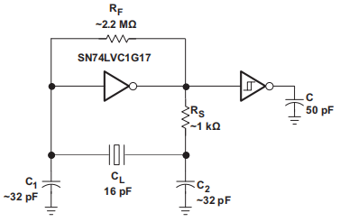
Typical Application of SN74LVC1G17DCKR
Layout of SN74LVC1G17DCKR

Tying Unused Inputs to Defined Logic Levels
In electronic circuit design, all unused inputs in multiple-bit logic devices must be connected to a clearly defined logic level to prevent floating states. Floating states can trigger unpredictable behavior and even system failure, as unstable inputs can randomly fluctuate, affecting the overall circuit performance. To mitigate this issue, unused inputs should be connected directly to either GND (ground) or VCC (power supply).
Grounding Unused Inputs for Stability
Grounding unused inputs stabilizes the circuit and diminishes noise and potential interference that might otherwise affect other parts of the system. When an unused input is unconnected, it can act as an antenna, picking up electromagnetic interference (EMI) from the environment. This interference can propagate through the device and lead to erroneous logic responses. Tying these inputs to GND minimizes the risk of such disturbances.
Effective Connection to VCC
Connecting unused inputs to VCC provides stable logic states. This method ensures that floating inputs maintain a constant high logic level, which is beneficial in certain circuit setups where a default high state is desired. However, it is good to verify that the logic devices being used can safely handle the direct connection to VCC without exceeding their voltage tolerance limits. Consistent application of this technique enhances system reliability in complex digital circuits.
Applications of SN74LVC1G17DCKR
AV Receivers
AV receivers handle audio and video signals in enriching home entertainment systems. They create a captivating atmosphere with surround sound and high-definition visuals. Mastery of input/output configurations and system compatibility contributes to their optimized use.
Portable Audio Docks
Portable audio docks epitomize convenience by enabling easy connections to various devices, perfect for casual listening or outdoor festivities. Emphasis on battery life and Bluetooth connectivity shows their practical appeal, ensuring uninterrupted enjoyment wherever you go.
Blu-ray Players and Home Theaters
Blu-ray players and home theaters bring forth the magic of cinema into domestic settings with stunning high-definition video and immersive soundscapes. The adoption of advancements such as 4K resolution and Dolby Atmos has not just improved but transformed viewing, making each moment memorable.
MP3 Players/Recorders
For music aficionados who seek portable and intimate audio, MP3 players and recorders prove importance. The push for larger storage capacities and superior sound quality remains, with an added emphasis on compatibility with diverse audio formats, catering to a personalized soundtrack of life.
PDAs
Personal Digital Assistants (PDAs) function as versatile devices that streamline both business and personal activities. The advent of touchscreens and wireless communication features has broadened their scope from basic task management to sophisticated operational capabilities, enhancing productivity.
Telecom/Server Power Supplies
Telecom and server power supplies ensure the robustness of network and data center operations. Efficiency and sustainability play a role, with innovative design techniques focusing on energy reduction and improved thermal management. Reliability in these systems prevents downtime and maintains seamless connectivity.
SSDs (Client and Enterprise)
Solid State Drives (SSDs) revolutionize data storage performance across personal and enterprise contexts. They deliver faster access speeds, exceptional reliability, and durability for workflows demanding high efficiency. Their deployment can dramatically elevate the operational tempo.
LCD/HDTVs
LCD and HDTVs continue to captivate with their vivid visual performance and energy-saving attributes. Cutting-edge technologies, like OLED and QLED, offer enriched contrast and color precision, drawing towards superior visual that redefine vividness on screen.
Enterprise Tablets
Enterprise tablets bolster efficiency with their blend of portability and computing prowess. In sectors spanning healthcare to logistics, they gain widespread use due to their long battery life, robust security features, and multitasking capability, proving to be versatile tools in various landscapes.
Video Analytics Servers
Video analytics servers play a role in processing extensive video data for uses including security, traffic management, and retail analysis. Effective performance hinges on robust hardware setups, sophisticated software algorithms, and the ability for data processing, enabling insightful analysis and prompt decision-making.
Wireless Headsets, Keyboards, and Mice
Wireless peripherals like headsets, keyboards, and mice enhance flexibility and comfort. Advances such as Bluetooth Low Energy technology have boosted battery efficiency and connectivity reliability.
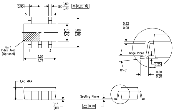
Package of SN74LVC1G17DCKR
Manufacturer of SN74LVC1G17DCKR
Texas Instruments Inc. (TI), a name synonymous with pioneering advancements, has firmly established itself in the semiconductor and integrated circuit (IC) manufacturing industry. Originating as Geophysical Service Incorporated (GSI) in 1930, TI's rich history is a testament to its transformative journey. The restructuring in 1951 marked the emergence of the present-day TI, heralding an era characterized by relentless technological innovation and industry dominance. Texas Instruments Inc. epitomizes the transformative power of unwavering innovation. From its humble beginnings as Geophysical Service Incorporated to its current standing as a semiconductor titan, TI’s journey is a compelling narrative of continuous research and development. The company's sustained influence across various industries not only attests to its leading role but also reflects its enduring commitment to shaping a progressive technological future.
Datasheet PDF
SN74LVC1G17DCKR Datasheets:
Copper Bond Wire 07/May/2014.pdf
Copper Wire Revision A 03/Nov/2014.pdf
Frequently Asked Questions [FAQ]
1. What does the Schmitt trigger do?
The Schmitt trigger proficiently eliminates noise from signals, adeptly managing mechanical contact bounce in switches. This function enhances the dependability of digital circuits by providing pristine signal transitions. Such clean signal transitions are great for applications including signal conditioning and debounce circuits.
2. What voltage range does it operate in?
The Schmitt trigger operates within a voltage spectrum of 1.65V to 5.5V Vcc, versatile enough to suit various systems. The expansive voltage range makes it compatible with different power supply requirements. This adaptability is notably advantageous in crafting versatile electronic devices, particularly those demanding both low-power and high-performance features.
3. What is its Boolean operation?
The Boolean function is represented as Y = A. This direct logical relationship ensures that the output mirrors the input when processed through the Schmitt trigger. Predictable behavior in digital circuits is maintained, making circuit design straightforward by ensuring an unambiguous correlation between input and output.
4. What is its output drive capability?
It boasts high output drive capability across a broad Vcc range, making it adept at driving various loads. This efficient drive ability means the component is fitting for diverse applications, from simple LED indicators to intricate microcontroller interfaces. This reliability is appealing in tasks requiring steadfast output performance.
5. What is the body size of its compact DPW package?
The dimensions of the compact DPW package are 0.8 mm x 0.8 mm. Such a diminutive footprint is advantageous for integration into modern, space-constrained electronics. The compact size does not compromise the functionality in the development of dense, feature-abundant devices like wearable technology and compact IoT sensors.
6. Why does it work as a standalone buffer?
The Schmitt trigger's inherent Schmitt action enables it to function efficaciously as a standalone buffer by providing hysteresis that stabilizes the output against small, fluctuating input signals. This characteristic is good for preventing false triggering and achieving stable output levels, rendering it a reliable component in digital system designs.
7. What is the DPW package technology’s importance?
DPW package technology epitomizes advanced IC packaging, offering benefits including reduced parasitic effects and enhanced thermal performance. These attributes are excellent in augmenting the electrical performance and reliability of integrated circuits, particularly important as electronic devices continue to diminish in size while demanding higher efficiency.
8. What is the DPW package's footprint size?
The footprint of the DPW package is minimal, at 0.64 mm². This compact footprint is conducive to creating high-density electronic assemblies for the miniaturization trends seen in electronics, medical devices, and other cutting-edge industries.
9. What type of applications is it suitable for?
It excels in partial-power-down applications for conserving energy and maintaining specific circuit functionalities during low power states. This trait is use in energy-saving designs and applications requiring low-power operation, such as battery-powered devices and energy-efficient computing systems.
10. What disables the outputs?
The Ioff circuitry is what disables the outputs. This mechanism plays a role in managing power consumption and safeguarding the circuit during power-down states, ensuring that undesired operations are off-limits. Such a feature contributes to prolonging battery life and enhancing overall system stability.
About us
ALLELCO LIMITED
Read more
Quick inquiry
Please send an inquiry, we will respond immediately.
CR1220 Lithium Coin Battery: Specifications, Equivalent, and Datasheet
on October 18th
TL074ID Op-Amp: Features, Applications, and Datasheet
on October 17th
Popular Posts
-
What is GND in the circuit?
on January 1th 3282
-

RJ-45 Connector Guide: RJ-45 Connector Color Codes, Wiring Schemes, R-J45 Applications, RJ-45 Datasheets
on January 1th 2817
-
Understanding Power Supply Voltages in Electronics VCC, VDD, VEE, VSS, and GND
on November 20th 2662
-

Fiber Connector Types: SC Vs LC And LC Vs MTP
on January 1th 2269
-

Comparison Between DB9 and RS232
on January 1th 1886
-

What Is An LR44 Battery?
Electricity, that ubiquitous force, quietly permeates every aspect of our daily lives, from trivial gadgets to life-threatening medical equipment, it plays a silent role. However, truly grasping this energy, especially how to store and efficiently output it, is no easy task. It is against this background that this article will focus on a type of coin cell battery that may seem insignificant on the...on January 1th 1847
-
What Is RF and Why Do We Use It?
Radio Frequency (RF) technology is a key part of modern wireless communication, enabling data transmission over long distances without physical connections. This article delves into the basics of RF, explaining how electromagnetic radiation (EMR) makes RF communication possible. We will explore the principles of EMR, the creation and control of RF signals, and their wide-ranging uses. The article ...on January 1th 1812
-
Understanding the Fundamentals:Inductance Resistance, andCapacitance
In the intricate dance of electrical engineering, a trio of fundamental elements takes center stage: inductance, resistance, and capacitance. Each bears unique traits that dictate the dynamic rhythms of electronic circuits. Here, we embark on a journey to decipher the complexities of these components, to uncover their distinct roles and practical uses within the vast electrical orchestra. Inductan...on January 1th 1811
-
CR2430 Battery Comprehensive Guide: Specifications, Applications and Comparison to CR2032 Batteries
What is CR2430 battery ?Benefits of CR2430 BatteriesNormCR2430 Battery ApplicationsCR2430 EquivalentCR2430 VS CR2032Battery CR2430 SizeWhat to look for when buying the CR2430 and equivalentsData Sheet PDFFrequently Asked Questions Batteries are the heart of small electronic devices. Among the many types available, coin cells play a crucial role, commonly found in calculators, remote controls, and ...on January 1th 1804
-
Comprehensive guide to hFE in transistors
Transistors are crucial components in modern electronic devices, enabling signal amplification and control. This article delves into the knowledge surrounding hFE, including how to select a transistor's hFE value, how to find hFE, and the gain of different types of transistors. Through our exploration of hFE, we gain a deeper understanding of how transistors work and their role in electronic circu...on November 20th 1788
