Exploring the LF356 Op-Amp: Pinout and Package Specifications
The LF356 operational amplifier represents a remarkable blend of high-voltage JFETs and standard bipolar transistors on a single chip, setting it apart in the world of high-performance op-amps. This unique integration leverages the low input bias currents and high input impedance of JFETs with the strength and speed of bipolar transistors, making the LF356 an ideal choice for complex electronic systems requiring precision and responsiveness. Whether used in high-impedance buffering, wideband amplification, or precision instrumentation, the LF356 offers you a versatile and reliable solution. This article explores its packaging, pin configuration, technical specifications, and key applications, showcasing why the LF356 is a preferred tool in advanced electronic design.Catalog
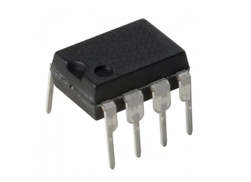
Overview of the LF356
The LF356 represents a noteworthy evolution in the world of monolithic JFET input operational amplifier technology. By integrating high-voltage JFETs with conventional bipolar transistors through BI-FET™ Technology, it achieves remarkable performance traits. For example, it maintains an impressively low input bias and offset current, alongside reduced offset voltage and drift. Its offset adjustment feature allows for stable drift and common-mode rejection ratios. It also boasts a high slew rate, expansive bandwidth, and swift settling time. Additionally, the design significantly diminishes noise levels and showcases a low 1/f noise corner.
The LF356's architecture emphasizes fine-tuning various factors in operational amplifiers. Utilizing matched high-voltage JFETs with standard bipolar transistors via BI-FET™ Technology, the device excels in delivering superior input characteristics. Among these are exceptionally low input bias and offset currents, instrumental for accuracy in exacting applications. The minimal offset voltage and drift, beneficial for sustained stability, work in tandem with adjustable offset capabilities, enabling the device to uphold its drift and common-mode rejection performance across diverse operational contexts.
From practical experience, devices like the LF356 are known to thrive in scenarios where precision and stability are deeply valued. Its high slew rate and vast bandwidth are mostly advantageous for high-speed analog computing and signal processing, making it a preferred choice in such areas. Laboratories frequently depend on these amplifiers for exact and dependable outcomes. Moreover, the rapid settling time is especially advantageous in data acquisition systems, where prompt response and precision hold great significance. The reduced voltage/current noise and low 1/f noise corner further enhance its fit for high-fidelity audio and instrumentation applications, where safeguarding signal purity is highly valued.
LF356 Pin Configuration
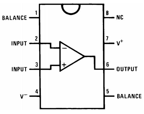
|
PIN NAME |
PIN NO. |
I/O |
DESCRIPTION |
|
BALANCE |
1, 5 |
I |
Balance for input offset voltage |
|
+INPUT |
3 |
I |
Noninverting input |
|
–INPUT |
2 |
I |
Inverting input |
|
NC |
8 |
— |
No connection |
|
OUTPUT |
6 |
O |
Output |
|
V+ |
7 |
— |
Positive power supply |
|
V– |
4 |
— |
Negative power supply |
LF356 CAD Model Analysis
Electrical Symbol
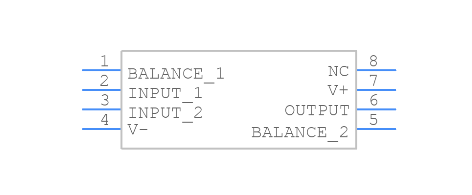
PCB Footprint

Three-Dimensional Model
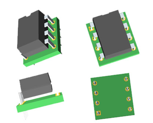
Features
|
Feature |
Description |
|
Hybrid & Module Replacement |
Replaces expensive hybrid and module FET op amps |
|
JFET Durability |
Uses rugged JFETs for blow-out-free handling compared to
MOSFET input devices |
|
Low Noise Performance |
Excellent for low noise applications with both high and
low source impedance; very low 1/f corner |
|
Offset Adjustment Stability |
Offset adjustment does not degrade drift or common-mode
rejection as seen in most monolithic amplifiers |
|
Large Capacitive Load Handling |
New output stage supports large capacitive loads (up to
5,000 pF) without stability issues |
|
Internal Compensation & High Differential Input
Capability |
Provides internal compensation and supports large
differential input voltage |
Technical Specifications
Here is the table format for the technical specifications and attributes of the Texas Instruments LF356N.
|
Type |
Parameter |
|
Mount |
Through Hole |
|
Mounting Type |
Through Hole |
|
Package / Case |
8-DIP (0.300, 7.62mm) |
|
Number of Pins |
8 |
|
Operating Temperature |
0°C ~ 70°C |
|
Packaging |
Tube |
|
Series |
BI-FET™ |
|
JESD-609 Code |
e0 |
|
Pbfree Code |
No |
|
Part Status |
Obsolete |
|
Moisture Sensitivity Level (MSL) |
1 (Unlimited) |
|
Number of Terminations |
8 |
|
ECCN Code |
EAR99 |
|
Terminal Finish |
Tin/Lead (Sn/Pb) |
|
Packing Method |
RAIL |
|
Max Power Dissipation |
670mW |
|
Terminal Position |
DUAL |
|
Number of Functions |
1 |
|
Supply Voltage |
15V |
|
Terminal Pitch |
2.54mm |
|
Base Part Number |
LF356 |
|
Pin Count |
8 |
|
Operating Supply Voltage |
15V |
|
Number of Channels |
1 |
|
Operating Supply Current |
5mA |
|
Nominal Supply Current |
5mA |
|
Power Dissipation |
670mW |
|
Output Current |
25mA |
|
Max Supply Current |
10mA |
|
Slew Rate |
12V/μs |
|
Architecture |
VOLTAGE-FEEDBACK |
|
Amplifier Type |
J-FET |
|
Common Mode Rejection Ratio |
80 dB |
|
Current - Input Bias |
30pA |
|
Voltage - Supply, Single/Dual (±) |
±15V |
|
Input Offset Voltage (Vos) |
10mV |
|
Neg Supply Voltage-Nom (Vsup) |
-15V |
|
Unity Gain BW-Nom |
5000 kHz |
|
Voltage Gain |
106.02dB |
|
Average Bias Current-Max (IIB) |
0.0002μA |
|
Power Supply Rejection Ratio (PSRR) |
80dB |
|
Low-Offset |
No |
|
Frequency Compensation |
Yes |
|
Voltage - Input Offset |
3mV |
|
Low-Bias |
Yes |
|
Bias Current-Max (IIB) @25C |
0.0002μA |
|
Input Offset Current-Max (IIO) |
0.002μA |
|
Height |
3.3mm |
|
Length |
9.27mm |
|
Width |
6.35mm |
|
REACH SVHC |
No SVHC |
|
Radiation Hardening |
No |
|
RoHS Status |
Non-RoHS Compliant |
|
Lead Free |
Contains Lead |
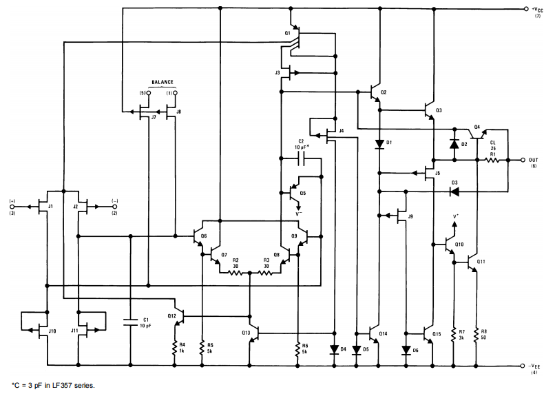
Functional Block Diagram
Modern Applications of the LF356
The LF356 operational amplifier flourishes in a domain that demands both acute precision and rapid responsiveness. Its utility as a component in high-speed integrators is notable, as it adeptly processes swift signal changes with minimal delay. In the sphere of D/A and A/D converters, the LF356 adeptly manages digital-to-analog and analog-to-digital transformations, playing a prominent role in digital signal processing frameworks and communication systems.
High Impedance Buffers
In scenarios demanding high impedance buffering, the LF356 upholds signal integrity across multiple transmission contexts. Used in sensor interfacing or driver stages, the LF356 provides stable buffers, enhancing overall system performance.
Wideband Amplifiers
The LF356's reach extends to wideband amplifier applications, where its extensive frequency response range is highly valued. In radio frequency communications and broadcast equipment, the LF356 ensures robust signal amplification, maintaining both speed and quality, showcasing meticulous engineering throughout.
Low Noise and Drift Applications
In pursuits where minimal noise interference and drift are key, such as sensitive audio equipment or exacting measurement tools, the LF356 shines. Its low noise contributions are mostly requisite in environments where even trivial levels of interference could be disruptive, embodying the continuous effort to further refine engineering.
Specialized Logarithmic and Photocell Amplifiers
Logarithmic and photocell amplifier configurations benefit greatly from the LF356’s stability and responsiveness to varying light levels or exponential tasks. Applications in optical sensing and sophisticated computational work illustrate how the LF356 provides a dependable performance baseline, fostering innovations in light-sensitive technology.
Efficient Sample and Hold Circuits
In sample and hold circuits, the LF356 excels, skillfully capturing and maintaining precise signal values. This role is major in digital systems where the timing and accuracy of data are of notable importance. Practical uses include various instruments and digital modulation systems that rely on the fidelity of a momentary signal snapshot to maintain process integrity.
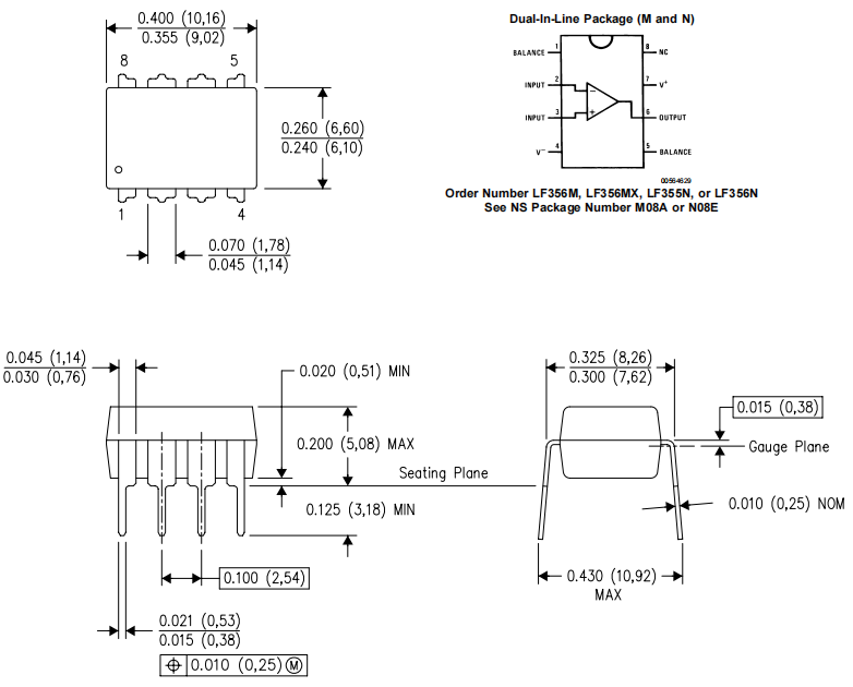
Package
Manufacturer
Texas Instruments (TI) traces its esteemed legacy in semiconductor technology back to 1958 when it pioneered the creation of the first working integrated circuit. Today, with a workforce exceeding 30,000 worldwide, TI remains a leader in pushing the boundaries of innovation, especially in the promising areas of analog and embedded processing sectors. The company's dedication to solving challenges through collaboration is a driving force propelling technological advancements on a global scale.
About us
ALLELCO LIMITED
Read more
Quick inquiry
Please send an inquiry, we will respond immediately.
Frequently Asked Questions [FAQ]
1. What op-amp (the LM741 or the LF356) is closest to an ideal op-amp, and why?
When examining the ideal operational amplifier qualities, the LF356 distinctly surpasses the LM741. This advantage stems from the LF356's FET input, which markedly lowers the input current. It boasts an enhanced slew rate. These characteristics advocate for the LF356's adoption in diverse applications, mostly those requiring optimal management of input impedance and frequency response. You can often favor the LF356 for high-performance circuits, leveraging its reliability and efficiency in complex signal processing. The subtleties of these performance parameters lie in the detailed analysis of circuit design objectives and the specific application demands.
2. How can I get the maximum output voltage of an op-amp knowing the input voltage, specifically an LF356?
The determination of the LF356's maximum output voltage involves several intersecting factors input voltage and gain, as modulated by external components. Supply voltage and inherent voltage swings per its datasheet specifications. Typically, you can anticipate ±13V with a ±15V supply into a 10k load, or a ±12V outcome at a 2k load. Understanding the interplay between these variables guides you to optimize circuit efficiency and output performance. Hands-on experiences reveal the importance of careful parameter balancing when approaching complex voltage regulations.
3. Why isn't my LF356 op-amp rail-to-rail? Even if the load impedance is 10M ohm, the output voltage is like a volt off.
The LF356 is structurally precluded from achieving rail-to-rail output due to its output stage. Engineered with NPN transistors configured in a Darlington pair. This arrangement yields a voltage drop roughly twice the base-emitter junction's voltage decline, around 1.3V. This characteristic necessitates consideration when selecting op-amps for applications where output voltage proximity to supply rails is used. Exact comprehension of the transistor-level operation aids in selecting apt components while accommodating design constraints.
4. Which op-amp (the LM741 or LF356) is better suited for high-frequency signals in terms of bandwidth?
The LF356, endowed with a 5MHz gain bandwidth product (GBW), distinctly outperforms the LM741's 1MHz GBW rendering it more suitable for high-frequency applications. You can recognize evolving technological demands might gravitate towards contemporary op-amps when the operating voltage range permits flexibility. Years of iterative design and testing affirm that embracing modern solutions can enhance signal fidelity and operational bandwidth in cutting-edge technological projects. This forward-thinking integration of modern components aligns with the pursuit of enhanced precision in electronic applications.
LD1117 Voltage Regulator: Pinout, Alternatives, and Specifications
on November 5th
Exploring the Features and Performance of the W5500 Hardwired TCP/IP Controller
on November 4th
Popular Posts
-
What is GND in the circuit?
on January 1th 2915
-

RJ-45 Connector Guide: RJ-45 Connector Color Codes, Wiring Schemes, R-J45 Applications, RJ-45 Datasheets
on January 1th 2477
-

Fiber Connector Types: SC Vs LC And LC Vs MTP
on January 1th 2064
-
Understanding Power Supply Voltages in Electronics VCC, VDD, VEE, VSS, and GND
on November 8th 1857
-

Comparison Between DB9 and RS232
on January 1th 1749
-

What Is An LR44 Battery?
Electricity, that ubiquitous force, quietly permeates every aspect of our daily lives, from trivial gadgets to life-threatening medical equipment, it plays a silent role. However, truly grasping this energy, especially how to store and efficiently output it, is no easy task. It is against this background that this article will focus on a type of coin cell battery that may seem insignificant on the...on January 1th 1702
-
Understanding the Fundamentals:Inductance Resistance, andCapacitance
In the intricate dance of electrical engineering, a trio of fundamental elements takes center stage: inductance, resistance, and capacitance. Each bears unique traits that dictate the dynamic rhythms of electronic circuits. Here, we embark on a journey to decipher the complexities of these components, to uncover their distinct roles and practical uses within the vast electrical orchestra. Inductan...on January 1th 1647
-

CR2430 Battery Comprehensive Guide: Specifications, Applications and Comparison to CR2032 Batteries
What is CR2430 battery ?Benefits of CR2430 BatteriesNormCR2430 Battery ApplicationsCR2430 EquivalentCR2430 VS CR2032Battery CR2430 SizeWhat to look for when buying the CR2430 and equivalentsData Sheet PDFFrequently Asked Questions Batteries are the heart of small electronic devices. Among the many types available, coin cells play a crucial role, commonly found in calculators, remote controls, and ...on January 1th 1532
-
What Is RF and Why Do We Use It?
Radio Frequency (RF) technology is a key part of modern wireless communication, enabling data transmission over long distances without physical connections. This article delves into the basics of RF, explaining how electromagnetic radiation (EMR) makes RF communication possible. We will explore the principles of EMR, the creation and control of RF signals, and their wide-ranging uses. The article ...on January 1th 1521
-

CR2450 vs CR2032: Can The Battery Be Used Instead?
Lithium manganese batteries do have some similarities with other lithium batteries. High energy density and long service life are the characteristics they have in common. This kind of battery has won the trust and favor of many consumers because of its unique safety. Expensive tech gadgets? Small appliances in our homes? Look around and you'll see them everywhere. Among these many lithium-manganes...on January 1th 1496


