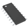
CD4007 CMOS Inverter: Pinout, Datasheet, and 14-SOIC Package Overview
The CD4007 is a versatile integrated circuit (IC) that integrates a dual complementary pair of MOSFET transistors and an inverter stage, making it a valuable asset in both analog and digital circuit designs. Its flexible configuration and strong performance characteristics allow it to be widely used across various applications. In this article, we will dig into the basic aspects of the CD4007, including its pinout, key features, and practical applications. In addition, we’ll provide insights into actual usage, production considerations, and a detailed overview of its datasheet, offering a comprehensive guide for you to utilize this IC effectively in your designs.Catalog
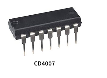
Understanding the CD4007 IC
The CD4007 Integrated Circuit (IC) is a basis in contemporary electronics due to its composition of three pairs of complementary N-channel and P-channel MOS transistors. These transistor pairs offer remarkable versatility, as they can be utilized in both series and shunt configurations, providing tailored solutions for various circuit design needs. Moreover, the CD4007 interfaces effortlessly with several types of devices.
• CMOS (Complementary Metal-Oxide-Semiconductor)
• NMOS (N-channel Metal-Oxide-Semiconductor)
• TTL (Transistor-Transistor Logic)
The CD4007 glows in scenarios requiring low thermal dissipation and substantial noise immunity. It expertly manages voltage levels, keeping them between the supply voltage (VDD) and ground (VSS) within a narrow 0.3V margin. This precise voltage control is instrumental in applications that prioritize minimizing power loss and sustaining signal integrity.
The IC's steadfast protection against electrostatic discharge (ESD) is another notable attribute. Analyzing the detrimental effects of ESD on electronic components, the CD4007 comes equipped with clamping diodes between the voltage drain (VD) and ground (VSS). These diodes promptly absorb sudden voltage spikes, safeguarding the inputs from static electricity, a major feature for components regularly exposed to variable static conditions during handling and operation.
CD4007 Pin Configuration
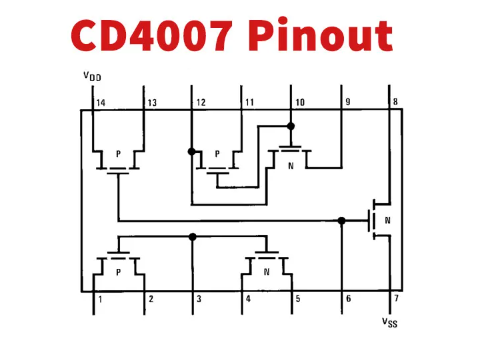
|
Pin No |
Pin Name |
Description |
|
1 |
2Dp |
The drain of p Channel 2 |
|
2 |
2Sp |
Source of p Channel 2 |
|
3 |
2A |
Input Channel 2 |
|
4 |
2Sn |
Source of n Channel 2 |
|
5 |
2Dn |
The drain of n Channel 2 |
|
6 |
1A |
Input Channel 1 |
|
7 |
VSS |
Source Supply |
|
8 |
1Dn |
The drain of n Channel 1 |
|
9 |
3Sn |
Source of n Channel 3 |
|
10 |
3A |
Input Channel 3 |
|
11 |
3Sp |
Source of p Channel 3 |
|
12 |
3Y |
Output |
|
13 |
1Dp |
The drain of p Channel 1 |
|
14 |
VDD |
Drain Supply |
CAD Model of CD4007
CD4007 Footprint
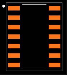
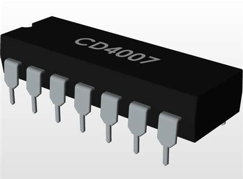
CD4007 3D Model
Specifications of CD4007
|
Type |
Parameter |
Value |
|
Mount |
Mounting Type |
Surface Mount |
|
Package / Case |
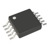
14-SOIC (0.154, 3.90mm Width) |
|
|
Number of Pins |
14 |
|
|
Supplier Device Package |
14-SOIC |
|
|
Operating Conditions |
Operating Temperature |
-40°C to 85°C |
|
Max Operating Temperature |
85°C |
|
|
Min Operating Temperature |
-40°C |
|
|
Electrical Characteristics |
Supply Voltage |
3V to 15V |
|
Max Supply Voltage |
15V |
|
|
Min Supply Voltage |
3V |
|
|
Propagation Delay |
50 ns |
|
|
Design Specifications |
Series |
4000B |
|
Logic Function |
Inverter |
|
|
Logic Type |
Complementary Pair Plus Inverter |
|
|
Number of Circuits |
2 |
|
|
Number of Bits |
3 |
|
|
Number of Input Lines |
3 |
|
|
Number of Output Lines |
3 |
|
|
Base Part Number |
4007 |
|
|
Polarity |
Inverting |
|
|
Additional Details |
Packaging |
Tube |
|
Part Status |
Obsolete |
|
|
Moisture Sensitivity Level (MSL) |
1 (Unlimited) |
|
|
RoHS Status |
RoHS Compliant |
|
|
Lead Free |
Lead Free |
|
|
Published |
1999 |
Features of CD4007
|
Feature |
Description |
|
Wide supply voltage range |
3.0V to 15V |
|
High noise immunity |
0.45 VCC (Typ.) |
|
Quiescent current testing |
100% tested at 20V |
|
Symmetrical output characteristics |
Standardized, ensuring reliable output |
Applications of CD4007
The CD4007 integrated circuit, known for its adaptability and dependable performance, finds diverse applications across various electronic designs.
Precision Signal Sharpeners
The CD4007 is adept in constructing signal sharpening circuits, a needed component of digital systems where precise signal edges are authoritative for accurate timing and functionality. These sharpeners refine noisy signals into clean, well-defined pulses, used in communication systems to avoid timing errors and data corruption. You can observe that incorporating the CD4007 enhances signal integrity, ensuring stable data transmission.
Efficient Digital Inverters
In the world of digital electronics, inverters serve as ultimate components. When configured correctly, the CD4007 functions as a highly efficient inverter, admired for its low power consumption and robust performance, making it ideal for large-scale integration applications. You can notice that the CD4007 provides consistent performance in complex logic circuits and microprocessors, significantly contributing to circuit stability and reliability in digital logic design.
Accurate Threshold Detectors
Threshold detectors determine whether an input signal surpasses a specific value and are active in automation and safety systems. By using the CD4007, these detectors operate with high precision and minimal component count. This efficiency is mostly valued in control systems where accurate threshold detection ensures appropriate system responses to varying input levels. Actual applications showcase the CD4007 enhancing operational safety and efficiency with reliable threshold detection.
High-Fidelity Linear Amplifiers
Linear amplifiers amplify small signals without waveform distortion, and the CD4007, when configured as a linear amplifier, provides stable and pristine signal amplification. This is dominant in audio and instrumentation applications where signal fidelity is serious. You can appreciate the CD4007 for maintaining signal integrity throughout amplification, thus supporting its indispensability in sensitive analog circuitry.
Stable Crystal Oscillators
Crystal oscillators, which depend on stable frequency output through controlled crystal oscillations, frequently employ the CD4007 for maintaining consistency in oscillation parameters. This stability is active in timing devices and communication equipment. You can leverage the CD4007 have successfully developed crystal oscillators that exhibit high stability, ensuring the reliability and accuracy insistent for precise electronic applications. Such stable oscillators play a key role in enhancing performance in these domains.
Generative Potential of the CD4007 Transistor Array for Inverter Creation
The CD4007 package boasts the capability to generate up to three inverters, offering a versatile tool for diverse circuit applications. The ultimate inverter setup involves connecting pins 8 and 13 for the output, with pin 6 acting as the input. Pin 14 (VDD) must be connected to the power supply. Pin 7 (VSS) should be linked to the ground. Additional inverters can be arranged to meet specific requirements.
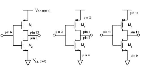
Pins 2 (VDD) and 4 (VSS) serve as the power connections. Pins 1 and 5 form the output. Pin 3 is the input. Pin 11 connects to VDD. Pin 9 is linked to VSS. Pin 12 serves as the output. Pin 10 provides the input.
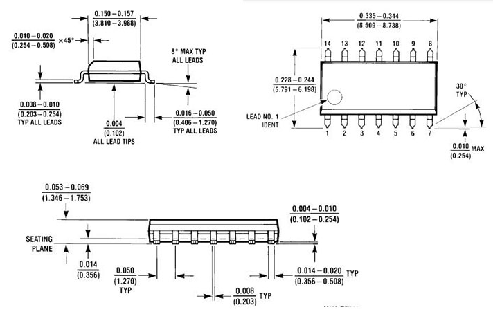
Dimensions of CD4007
Manufacturer of CD4007
ON Semiconductor (Nasdaq: ON) is renowned for its energy-efficient innovations, aiding global customers in their quest to reduce energy consumption. The company provides a vast array of solutions across various sectors, including automotive, communications, and consumer electronics.
The company's wide-reaching product range serves as a pillar of its market prominence. ON Semiconductor delivers adaptable and dependable solutions tailored to the unique demands of distinct industries. In the automotive sector, their products significantly enhance vehicle efficiency and safety leading to better fuel economy and ensuring a smoother and safer ride. In consumer electronics, the company's offerings are designed to maximize device performance and extend battery life.
ON Semiconductor's effective supply chain management guarantees the consistently timely availability of its products to meet global demand. The company's extensive network of facilities and offices, strategically placed in dangerous markets across North America, Europe, and Asia-Pacific, enables it to respond swiftly to market needs and customer requirements.
Parts with Similar Specs of CD4007
|
Part Number |
Manufacturer |
Package / Case |
Number of Pins |
Logic Function |
Number of Circuits |
Number of Output Lines |
Propagation Delay |
Min Supply Voltage |
Supply Voltage |
View Compare |
|
CD4007CM |
ON Semiconductor |
14-SOIC (0.154, 3.90mm Width) |
14 |
Inverter |
2 |
3 |
50 ns |
3 V |
3V ~ 15V |
CD4007CM |
|
MC14007UBD |
ON Semiconductor |
14-SOIC (0.154, 3.90mm Width) |
14 |
- |
- |
- |
18 ns |
- |
5 V |
MC14007UBD |
|
SN74HCT04DR |
Texas Instruments |
14-SOIC (0.154, 3.90mm Width) |
14 |
Inverter |
- |
- |
55 ns |
3 V |
3V ~ 18V |
SN74HCT04DR |
Datasheet PDF
CD4007CM Datasheets:
Cylindrical Battery Holders.pdf
MC14007UBD Datasheets:
SN74HCT04DR Datasheets:
Frequently Asked Questions [FAQ]
1. What can be CD4007 used for?
The CD4007 is a versatile IC that engineers can exploit for multiple purposes. It can form a chain of three inverters, an inverter with two transmission gates, or more complex logic gates. Inverters and transmission gates play a serious role in constructing digital systems such as D flip-flops. Recognizing the flexibility of the CD4007 enables you to design custom circuitry without the hassle of using multiple ICs. The capability to reconfigure the same IC for different uses not only conserves space on printed circuit boards but also streamlines the design process. This adaptability makes it a cherished tool in both academic and industrial environments.
2. What is the voltage of CD4007?
The CD4007 IC is often valued for its varied applications, low thermal dissipation, and impressive noise immunity. It operates between VSS at -0.3V and VDD at +0.3V. Proper voltage management is basic for maintaining the IC's integrity and extending its longevity. Ensuring these operational voltages are upheld is used to prevent electrical overstress that can degrade the IC's performance in sophisticated circuitry. Attention to this detail is mostly substantial during the prototyping phase of electronic design.
3. What is the circuit of CD4007?
Constructed using Metal Oxide Semiconductor (MOS) technology, the CD4007 is available in DIP and SOP packages. The IC includes three N-channel and three P-channel enhancement-type MOS transistors. This configuration is highly beneficial for developing both discreet and integrated logic circuits. Utilizing MOS technology offers the advantages of high input impedance and low power consumption. These benefits make the CD4007 a fitting choice for modern low-power applications. By making the most of the MOS transistors' properties, you can achieve circuits that are both efficient and reliable, mostly relevant in the age of portable and wearable electronic devices.
About us
ALLELCO LIMITED
Read more
Quick inquiry
Please send an inquiry, we will respond immediately.
Understanding the UA741IN Operational Amplifier
on October 21th
LM741 vs. LM358: Understanding the Differences for Optimal Selection
on October 21th
Popular Posts
-
What is GND in the circuit?
on January 1th 2915
-

RJ-45 Connector Guide: RJ-45 Connector Color Codes, Wiring Schemes, R-J45 Applications, RJ-45 Datasheets
on January 1th 2477
-

Fiber Connector Types: SC Vs LC And LC Vs MTP
on January 1th 2064
-
Understanding Power Supply Voltages in Electronics VCC, VDD, VEE, VSS, and GND
on November 8th 1860
-

Comparison Between DB9 and RS232
on January 1th 1749
-

What Is An LR44 Battery?
Electricity, that ubiquitous force, quietly permeates every aspect of our daily lives, from trivial gadgets to life-threatening medical equipment, it plays a silent role. However, truly grasping this energy, especially how to store and efficiently output it, is no easy task. It is against this background that this article will focus on a type of coin cell battery that may seem insignificant on the...on January 1th 1703
-
Understanding the Fundamentals:Inductance Resistance, andCapacitance
In the intricate dance of electrical engineering, a trio of fundamental elements takes center stage: inductance, resistance, and capacitance. Each bears unique traits that dictate the dynamic rhythms of electronic circuits. Here, we embark on a journey to decipher the complexities of these components, to uncover their distinct roles and practical uses within the vast electrical orchestra. Inductan...on January 1th 1647
-

CR2430 Battery Comprehensive Guide: Specifications, Applications and Comparison to CR2032 Batteries
What is CR2430 battery ?Benefits of CR2430 BatteriesNormCR2430 Battery ApplicationsCR2430 EquivalentCR2430 VS CR2032Battery CR2430 SizeWhat to look for when buying the CR2430 and equivalentsData Sheet PDFFrequently Asked Questions Batteries are the heart of small electronic devices. Among the many types available, coin cells play a crucial role, commonly found in calculators, remote controls, and ...on January 1th 1532
-
What Is RF and Why Do We Use It?
Radio Frequency (RF) technology is a key part of modern wireless communication, enabling data transmission over long distances without physical connections. This article delves into the basics of RF, explaining how electromagnetic radiation (EMR) makes RF communication possible. We will explore the principles of EMR, the creation and control of RF signals, and their wide-ranging uses. The article ...on January 1th 1521
-

CR2450 vs CR2032: Can The Battery Be Used Instead?
Lithium manganese batteries do have some similarities with other lithium batteries. High energy density and long service life are the characteristics they have in common. This kind of battery has won the trust and favor of many consumers because of its unique safety. Expensive tech gadgets? Small appliances in our homes? Look around and you'll see them everywhere. Among these many lithium-manganes...on January 1th 1496

