
Manufacturer Part Number
CDCLVD110AVF
Manufacturer
Texas Instruments
Introduction
High-performance clock distribution network component with LVDS capabilities.
Product Features and Performance
Fanout Buffer and Multiplexer functionality
Single circuit integration
2:10 input-to-output ratio
Supports differential signaling with LVDS
Maximum frequency handling capacity of 1.1 GHz
Operating voltage range of 2.375V to 2.625V
Operational temperature spectrum from -40°C to 85°C
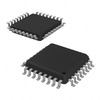
Surface mount 32-LQFP packaging
Enhanced signal integrity for high-speed applications
Product Advantages
Provides low jitter and skew distribution
Enables high-frequency clock signal distribution
Facilitates design flexibility with multiple outputs
Improved signal stability over a wide temperature range
Key Technical Parameters
1 GHz max frequency
Input and Output Differential LVDS signal support
375V to 2.625V supply voltage
2:10 input-to-output distribution ratio
32-LQFP package for compact mounting
Quality and Safety Features
Robust operational temperature range ensuring reliability
Conformance with industry quality standards
Compatibility
LVDS input compatible with common signaling standards
Multi-output compatible with a range of LVDS driven devices
Application Areas
Telecommunications
Data communications
High-speed computing systems
Industrial applications
Product Lifecycle
The product status is active
Not reported as nearing discontinuation
Potential availability of newer models or revisions
Several Key Reasons to Choose This Product
High speed and low-jitter performance
Scalability and versatility in application
Quality product from a reputable manufacturer
Long lifecycle with active product status
Designed for demanding high-performance environments


 CDCLVC1310RHBRTexas InstrumentsIC CLK BUFFER 3:10 200MHZ 32VQFN
 CDCLVD1208RHDRTexas InstrumentsIC CLK BUFFER 2:8 800MHZ 28VQFN
 CDCLVC1108PWRTexas InstrumentsIC CLK BUFFER 1:8 250MHZ 16TSSOP
 CDCLVD1204RGTTTexas InstrumentsIC CLK BUFFER 2:4 800MHZ 16VQFN