
Manufacturer Part Number
CDCLVC1310RHBR
Manufacturer
Texas Instruments
Introduction
High-performance CMOS clock buffer and distribution amplifier
Product Features and Performance
Supports a wide range of input signal types including HCSL, LVCMOS, LVDS, LVPECL, and SSTL
Provides 3 inputs to 10 LVCMOS outputs
Operates at up to 200 MHz
Differential input and output support
Low power consumption
Product Advantages
Wide input signal compatibility
High-speed operation up to 200 MHz
Flexible 3:10 input to output ratio
Differential signaling support
Low power design
Key Technical Parameters
Operating voltage: 2.375V to 3.465V
Operating temperature range: -40°C to 85°C
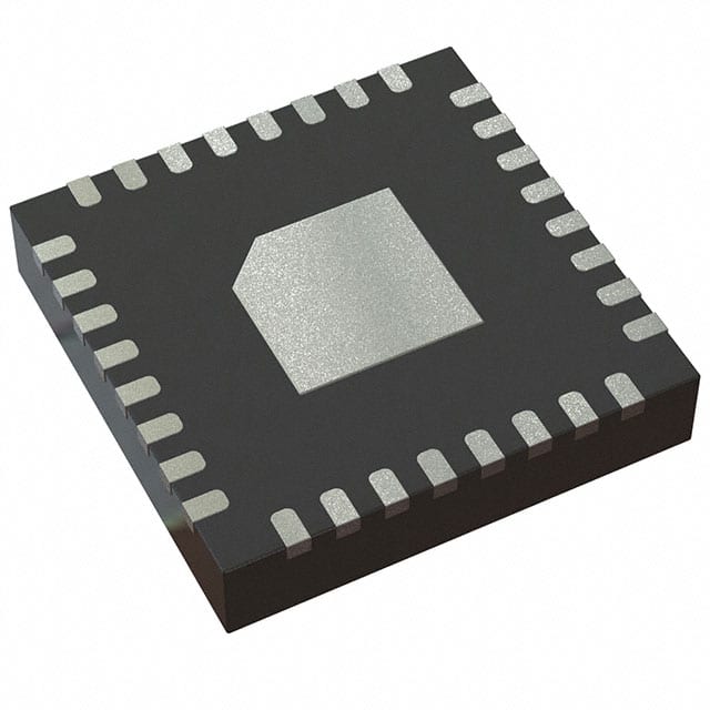
Package: 32-VQFN (5x5) with exposed pad
Quality and Safety Features
RoHS3 compliant
32-VQFN (5x5) package with exposed pad for enhanced thermal performance
Compatibility
Suitable for a wide range of digital system applications that require high-performance clock distribution
Application Areas
Networking and communications equipment
Servers and storage systems
Industrial and measurement equipment
Medical imaging systems
Product Lifecycle
This product is actively supported by Texas Instruments and is not nearing discontinuation.
Replacement or upgrade options may be available from Texas Instruments as technology evolves.
Key Reasons to Choose This Product
Wide input signal compatibility for design flexibility
High-speed operation up to 200 MHz for performance-critical applications
Flexible 3:10 input to output ratio for efficient clock distribution
Differential signaling support for improved signal integrity
Low power consumption for energy-efficient designs
RoHS3 compliance and thermal-enhanced package for quality and reliability


 CDCLVD1204RGTRTexas InstrumentsIC CLK BUFFER 2:4 800MHZ 16VQFN
 CDCLVD110VFTexas InstrumentsIC CLK BUFFER 2:10 1.1GHZ 32LQFP
 CDCLVC1106PWRTexas InstrumentsIC CLK BUFFER 1:6 250MHZ 14TSSOP
 CDCLVC1104PWRTexas InstrumentsIC CLK BUFFER 1:4 250MHZ 8TSSOP