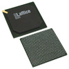
Manufacturer Part Number
LFE3-35EA-8FN484C
Manufacturer
Lattice Semiconductor
Introduction
The LFE3-35EA-8FN484C is an Embedded Field Programmable Gate Array (FPGA) produced by Lattice Semiconductor, designed for high-performance applications requiring a configurable logic solution.
Product Features and Performance
Includes 4125 Logic Array Blocks (LABs) and 33000 Logic Cells for extensive customization
Features 1,358,848 total RAM bits for robust data handling
Boasts 295 I/O pins for versatile connectivity options
Supports a voltage supply range from 1.14V to 1.26V
Operates within a temperature range of 0°C to 85°C
Product Advantages
High logic and I/O count increases applicability across various designs
Compact 484-FPBGA (23x23) packaging ideal for space-constrained applications
Offers a balance between performance and power consumption
Key Technical Parameters
Number of LABs/CLBs: 4125
Number of Logic Elements/Cells: 33000
Total RAM Bits: 1358848
Number of I/O: 295
Voltage Supply: 1.14V ~ 1.26V
Operating Temperature: 0°C ~ 85°C
Quality and Safety Features
Robust surface mount package ensures reliable soldering and secure mounting
Designed to meet stringent industry standards for performance stability and longevity
Compatibility
Compatible with various design and development tools offered by Lattice Semiconductor
Application Areas
Suitable for telecommunications, automotive, industrial, and consumer electronics applications
Product Lifecycle
Currently has an active product status
No near-term discontinuation, replacements or upgrades anticipated
Several Key Reasons to Choose This Product
High customization capability due to extensive number of logic elements and I/O options
Durable design suitable for industrial applications
Optimal balance of power consumption and performance, suitable for a variety of applications
Active product lifecycle with comprehensive support and compatibility


 LFE3-35EA-7FTN256CLattice Semiconductor CorporationIC FPGA 133 I/O 256FTBGA