
Manufacturer Part Number
NB3V1104CDTR2G
Manufacturer
onsemi
Introduction
A Fanout Buffer for distributing clock/timing signals
Product Features and Performance
Fanout Buffer (Distribution)
Supports up to 250 MHz frequency
Single-ended LVCMOS input and output
1:4 input to output ratio
Compatible with 1.71V to 3.6V supply voltages
Operational over a wide temperature range of -40°C to 105°C
Product Advantages
Supports high-frequency clock distribution
Flexible voltage range for various applications
Robust temperature tolerance for industrial use
Key Technical Parameters
1 Circuit Configuration
No Differential Input/Output
LVCMOS Input Type
LVCMOS Output Type
Maximum Frequency of 250 MHz
Voltage Supply Range from 1.71V to 3.6V
Surface Mount Mounting Type
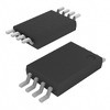
8-TSSOP Package
Quality and Safety Features
Designed for reliable performance across a wide operational temperature range
Comes in a standard package (TSSOP) known for stability
Compatibility
Compatible with LVCMOS signal levels
Industry-standard TSSOP format ensures compatibility with various PCB designs
Application Areas
Precision clock distribution in embedded systems
Telecommunications
Computing
Industrial electronics
Product Lifecycle
Product Status: Active
No indications of imminent discontinuation
Standard part with availability of replacement or potential future upgrades
Several Key Reasons to Choose This Product
High-frequency signal distribution capability
Versatility in power supply specifications
Enhanced performance in extreme temperature conditions
Ease of use in standard PCB designs
Reliable operation due to stringent quality measures
From a reputable manufacturer, onsemi, ensuring continuity of supply and support


 NB3N51034DTGonsemiIC CLK GEN CRYST1:4 HCSL 20TSSOP
 NB3N51032DTR2GonsemiIC CLOCK GENERATOR 16TSSOP
 NB3W1900LMNGonsemiIC CLOCK ZDB FANOUT BUFFER 72QFN
 NB3W1200LMNGonsemiIC CLK ZDB/FANOUT BUFFER 64QFN
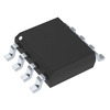 NB3N511DR2GonsemiIC CLOCK MULTIPLIER 8SOIC
 NB3V8312CMNGonsemiIC CLK BUFFER 1:12 250MHZ 32QFN
 NB3V8312CFAGonsemiIC CLK BUFFER 1:12 250MHZ 32LQFP