
Manufacturer Part Number
CDCVF25081PW
Manufacturer
Texas Instruments
Introduction
A versatile PLL Clock Driver designed for high-speed applications.
Product Features and Performance
-PLL feature with bypass option
-Inputs and outputs compatible with LVTTL levels
-Supports a single circuit but provides a 2:8 input-to-output ratio
-Operates at a frequency of up to 200MHz
-Supply voltage range from 3V to 3.6V
-Designed for surface mount technology
Product Advantages
-Enhanced signal integrity with LVTTL compatibility
-Flexibility in use due to PLL with bypass
-High output frequency range supports demanding applications
-Low voltage operation aids in reducing power consumption
-Simplified board design with surface mount package
Key Technical Parameters
-Type: PLL Clock Driver
-PLL: Yes, with Bypass
-Input: LVTTL
-Output: LVTTL
-Number of Circuits: 1
-Ratio - Input:Output: 2:8
-Differential - Input:Output: No/No
-Frequency - Max: 200MHz
-Voltage - Supply: 3V ~ 3.6V
-Operating Temperature: -40°C ~ 85°C
-Mounting Type: Surface Mount
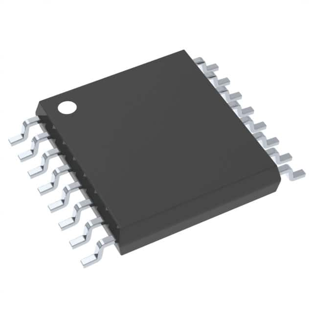
-Package / Case: 16-TSSOP
Quality and Safety Features
-Operates reliably within a wide temperature range (-40°C to 85°C)
Compatibility
-Designed for applications requiring LVTTL level inputs and outputs
Application Areas
-Suitable for high-frequency clock distribution in computing, telecommunications, and consumer electronics
Product Lifecycle
-Active product status indicates ongoing manufacturing and availability
-No current indication of discontinuation, replacements, or upgrades
Several Key Reasons to Choose This Product
-High-frequency operation up to 200MHz for speed-intensive applications
-Flexible power supply range (3V to 3.6V) for diverse power environments
-PLL with bypass option for versatile clock management
-Low operating temperature range supports use in challenging conditions
-Surface mount format for simplified PCB design and space-saving benefits


 CDCVF2505DRG4Texas InstrumentsIC PLL CLOCK DRIVER 8SOIC
 CDCVF2505PWG4Texas InstrumentsIC 3.3V PLL CLOCK-DRVR 8-TSSOP