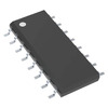
Manufacturer Part Number
CDC319DB
Manufacturer
Texas Instruments
Introduction
The CDC319DB is a fanout buffer designed for clock/timing signal distribution, particularly in applications requiring a 1:10 input-to-output ratio.
Product Features and Performance
Type: Fanout Buffer (Distribution), Data
Number of Circuits: 1
Input:Output Ratio of 1:10
Non-differential Input/Output
Input Type: LVTTL
Output Type: LVTTL, TTL
Maximum Frequency: 100 MHz
Operating Temperature Range: 0°C to 70°C
Mounting Type: Surface Mount
Package / Case: 28-SSOP
Product Advantages
Provides stable signal distribution with minimal signal degradation
Compatible with LVTTL and TTL output levels for increased versatility
Supports up to 100 MHz frequency for high-speed operations
Key Technical Parameters
Voltage Supply Range: 3.135V to 3.465V
Operates effectively within a 0°C to 70°C temperature range
Suitable for surface mount technology with a 28-SSOP package
Quality and Safety Features
Designed in compliance with industry standards for optimal reliability and safety
Performance tested across specified temperature and voltage ranges to ensure quality
Compatibility
Compatible with devices requiring LVTTL and TTL signal levels
Surface mount type ensures compatibility with modern PCB technologies
Application Areas
Primarily used in digital data transport systems
Suitable for electronics requiring precise clock/timing signal distribution
Product Lifecycle
Currently active and in production
No identified discontinuation in the near future, replacements or upgrades not specified
Several Key Reasons to Choose This Product
High fanout from a single input to ten outputs enhances circuit efficiency
Compatible with common logic levels (LVTTL/TTL) for broad application use
Reliable operation within standard industrial temperature ranges
Compact SSOP package favorable for space-constrained applications
Produced by Texas Instruments, a leader in semiconductor solutions


 CDC305-1NTexas Instruments
 CDC319DBRTexas InstrumentsIC CLK BUFFER 1:10 100MHZ 28SSOP