
Manufacturer Part Number
LCMXO2280C-3TN144C
Manufacturer
Lattice Semiconductor
Introduction
Lattice Semiconductor's LCMXO2280C-3TN144C is a high-performance, low-power FPGA (Field Programmable Gate Array) with a rich set of integrated features.
Product Features and Performance
2280 Logic Elements (LEs) for flexible and efficient logic implementation
28,262 Total RAM Bits for versatile data storage and processing
285 Logic Array Blocks (LABs) for configurable and scalable logic design
Supports operating voltages from 1.71V to 3.465V for wide range of applications
Operating temperature range of 0°C to 85°C for reliable performance in various environments
Product Advantages
Versatile FPGA solution with ample logic, memory, and I/O resources
Low-power design for energy-efficient operation
Flexible and reconfigurable architecture for adaptable system designs
Key Technical Parameters
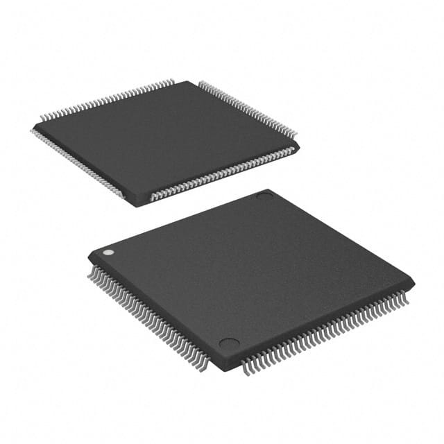
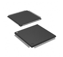
144-TQFP (20x20) package for compact integration
113 user I/O pins for extensive connectivity
RoHS3 compliant for environmentally-friendly applications
Quality and Safety Features
Robust design and manufacturing processes for reliable operation
Compliance with RoHS3 directives for hazardous substance reduction
Compatibility
Compatible with a wide range of Lattice Semiconductor's development tools and design software
Application Areas
Suitable for a variety of embedded systems, industrial automation, and consumer electronics applications
Product Lifecycle
The LCMXO2280C-3TN144C is an active product, with no immediate plans for discontinuation.
Replacement or upgrade options may be available within Lattice Semiconductor's FPGA portfolio.
Key Reasons to Choose This Product
Balanced performance and resource utilization for efficient system design
Low-power operation for energy-conscious applications
Flexible and reconfigurable architecture for adaptable solutions
Robust design and compliance with industry standards for reliable performance
Compatibility with Lattice Semiconductor's extensive ecosystem of development tools and software
 LCMXO2280C-3MN132ILattice Semiconductor CorporationIC FPGA 101 I/O 132CSBGA
 LCMXO2280C-3FTN256ILattice Semiconductor CorporationIC FPGA 211 I/O 256FTBGA
 LCMXO2280C-4FT256C-3ILattice Semiconductor
 LCMXO2280C-3TN100CLattice Semiconductor CorporationIC FPGA 73 I/O 100TQFP