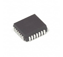
Manufacturer Part Number
MC88915TFN100R2
Manufacturer
NXP Semiconductors
Introduction
The MC88915TFN100R2 is a clock driver, fanout distribution, and multiplexer device from NXP Semiconductors. It features a PLL (Phase-Locked Loop) and supports TTL input and CMOS/TTL output signals. This device can be used in a variety of applications that require clock distribution and signal conditioning.
Product Features and Performance
PLL (Phase-Locked Loop) functionality
TTL input and CMOS/TTL output
1 circuit
3:8 input to output ratio
No differential input or output
Maximum frequency of 100MHz
Divider and multiplier capabilities
75V to 5.25V supply voltage
Operating temperature range of 0°C to 70°C
Surface mount package (28-LCC)
Product Advantages
Flexible clock distribution and signal conditioning capabilities
Supports a wide range of input and output signal types
Compact surface mount package for space-constrained designs
Wide operating voltage and temperature range
Key Reasons to Choose This Product
Reliable and robust clock management solution from a trusted semiconductor manufacturer
Versatile functionality to meet various system requirements
Cost-effective and space-efficient design
Proven performance in a wide range of applications
Quality and Safety Features
Rigorously tested for quality and reliability
Complies with industry safety standards
Compatibility
Suitable for a variety of digital and mixed-signal systems that require clock distribution and signal conditioning
Application Areas
Telecommunications equipment
Industrial control systems
Automotive electronics
Consumer electronics
Medical devices
Product Lifecycle
["The MC88915TFN100R2 is an obsolete product, meaning it is no longer in active production.","There may be equivalent or alternative models available from NXP Semiconductors or other manufacturers. Please contact our website's sales team for more information on the latest product options."]


 MC88915TMOTOROLA
 MC88916DW70NXP USA Inc.IC CLK BUF CISC 70MHZ 1CIRC
 MC88915TEI160Renesas Electronics America IncIC PLL CLOCK DRIVER 28PLCC