
Manufacturer Part Number
CY2308SXC-1
Manufacturer
Infineon Technologies
Introduction
The CY2308SXC-1 is a clock distribution chip designed to provide zero delay buffer and fanout capabilities.
Product Features and Performance
Fanout Buffer and Zero Delay Buffer
PLL circuit with Bypass option
Single-ended LVCMOS/LVTTL input compatible
LVCMOS level outputs
1-to-8 input-to-output ratio
Supports up to 133.3MHz frequency
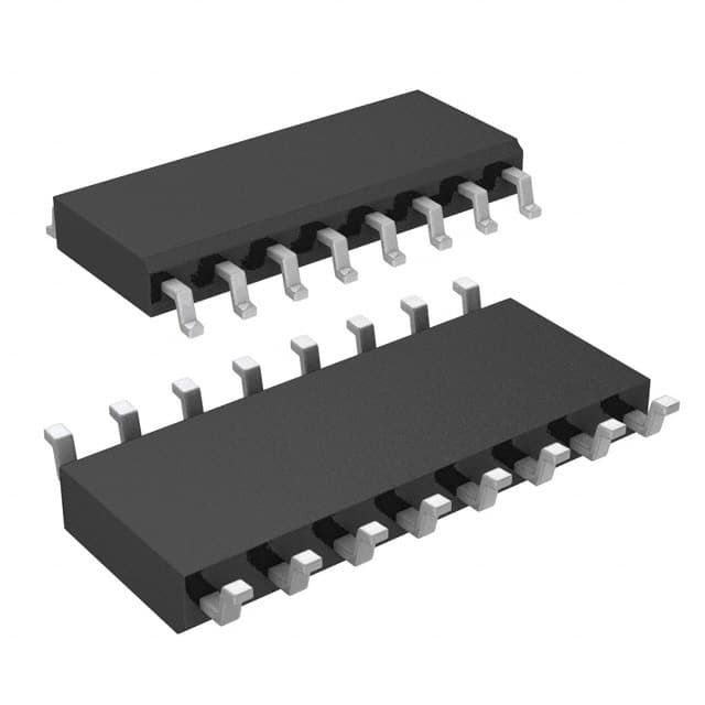
Surface Mount 16-SOIC package
3V to 3.6V supply voltage range
Operational temperature range from 0°C to 70°C
Product Advantages
Precision timing control
Minimal propagation delay
Allows for extensive distribution of a single clock source
Supports common signaling standards
Enhanced signal integrity due to low jitter and skews
Robust temperature performance for a wide range of applications
Key Technical Parameters
Type: Fanout Buffer/Zero Delay Buffer
PLL: Yes (with Bypass)
Input: LVCMOS, LVTTL
Output: LVCMOS
Number of Circuits: 1
Ratio - Input:Output: 1:8
Frequency - Max: 133.3MHz
Voltage - Supply: 3V ~ 3.6V
Operating Temperature: 0°C ~ 70°C
Quality and Safety Features
Manufactured to Infineon's quality standards
Designed for reliability and long operational life
Compatibility
Compatible with LVCMOS, LVTTL input standards
Standard surface mount packaging for compatibility with common PCB designs
Application Areas
Digital electronics
Communication systems
Data processing units
Consumer electronics
Industrial timing applications
Product Lifecycle
The CY2308SXC-1 is currently Active
No immediate risk of discontinuation
Check with Infineon Technologies for potential future upgrades or replacements
Several Key Reasons to Choose This Product
Highly reliable timing solution from a reputable manufacturer
Zero delay buffer ensures synchronization of downstream components
Eight outputs from a single input reduce component count
Suitable for high-frequency applications up to 133.3MHz
Operational across a broad voltage and temperature range
Ease of design integration thanks to standard SOIC package

 CY2308SC-4TCY
 CY2308SC-3TCypress Semiconductor CorpIC ZD BUFFER 16SOIC